
Method for fabricating flexible OLED display panel and flexible OLED display panel

A display panel, flexible technology, applied in the field of OLED display, can solve the problems of separation of OLED display unit 140, poor adhesion of thin film encapsulation layer 150, affecting product yield, etc.

Inactive Publication Date: 2019-11-19
SHENZHEN CHINA STAR OPTOELECTRONICS SEMICON DISPLAY TECH CO LTD
View PDF10 Cites 8 Cited by
  • Summary
  • Abstract
  • Description
  • Claims
  • Application Information

AI Technical Summary

Problems solved by technology

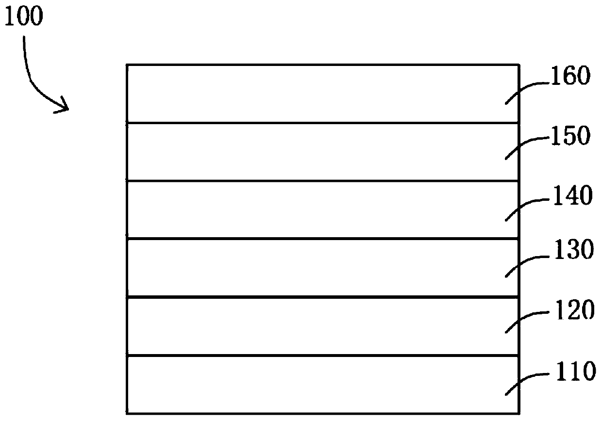
Please refer to figure 1 , wherein, in the prior art, after the thin film encapsulation is completed, the protective layer 160 will be laminated to prevent damage to the thin film encapsulation layer 150 in subsequent processes. Adhesion is not good, and the adhesion of the optically clear adhesive (optical clearadhesive, OCA) in the protective layer 160 is relatively large, which will easily cause the thin film encapsulation film layer 150 to separate from the OLED display unit 140 below it, seriously affecting product quality. Rate

Method used


Image

  • Method for fabricating flexible OLED display panel and flexible OLED display panel
  • Method for fabricating flexible OLED display panel and flexible OLED display panel
  • Method for fabricating flexible OLED display panel and flexible OLED display panel

Examples


Embodiment Construction

[0021] The following descriptions of the various embodiments refer to the accompanying drawings to illustrate specific embodiments that the present application can be used to implement. The directional terms mentioned in this application, such as [top], [bottom], [front], [back], [left], [right], [inside], [outside], [side], etc., are for reference only The orientation of the attached schema. Therefore, the directional terms used are used to illustrate and understand the application, but not to limit the application. In the figures, structurally similar elements are denoted by the same reference numerals.

[0022] Here, it should also be noted that, in order to avoid obscuring the present invention due to unnecessary details, only structures and / or processing steps closely related to the solution according to the present invention are shown in the drawings.

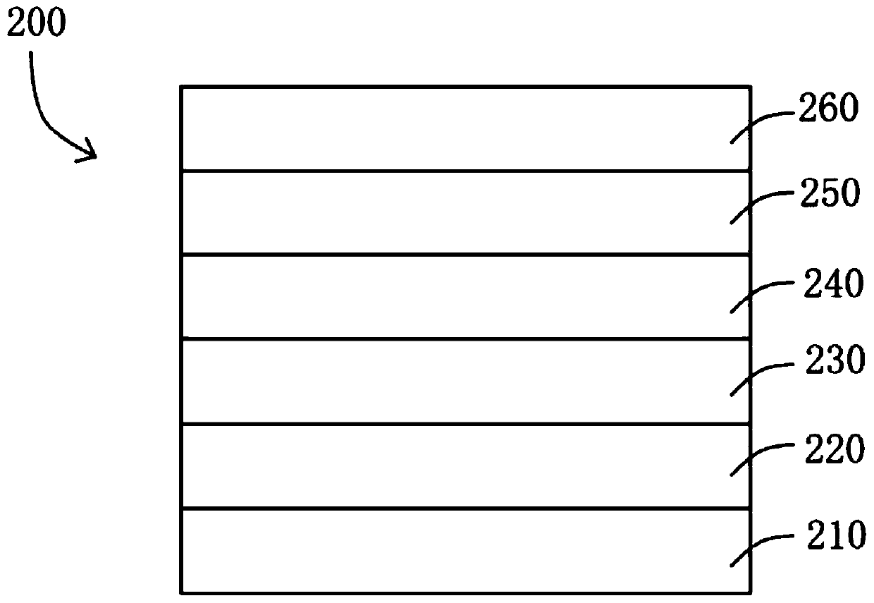
[0023] Please refer to figure 2 , figure 2 It is a schematic diagram of the structure before removing the protect...


PUM


Abstract

The present invention provides a method for fabricating a flexible OLED display panel, comprising a step S1 of providing a rigid substrate on which a flexible substrate is formed; a step S2 of forminga thin film transistor array layer on the flexible substrate; a step S3 of forming an OLED display unit on the thin film transistor array layer; a step S4 of forming an encapsulation layer on the OLED display unit; a step S5 of forming a protective layer on the encapsulation layer, wherein the protective layer is bonded to the surface of the encapsulation layer away from the surface of the OLED display unit by a heat-sensitive adhesive; a step S6 of peeling off the rigid substrate and attaching a support film to the bottom of the flexible substrate; a step S7 of removing the protective layer;and a step S8 of forming a protective cover plate on the encapsulation layer.

Description

technical field [0001] The invention relates to the field of OLED display technology, in particular to a method for preparing a flexible OLED display panel and the flexible OLED display panel. Background technique [0002] Organic light-emitting diode (OLED) is a self-luminous device with many advantages: active light emission, high luminous efficiency, high contrast, low power consumption, wide viewing angle, fast response speed, wide operating temperature range, light and thin, etc. , has become one of the most widely used display devices in recent years, and therefore, flexible OLED display panels using this light-emitting device have become mainstream products in the display field. [0003] The conventional flexible OLED (Flexible OLED) device manufacturing process usually includes the following main manufacturing processes: a flexible substrate is formed on a glass substrate, and then a thin-film transistor backplane, anode, pixel definition layer, and light-emitting la...

Claims


Application Information

Patent Timeline
Patent Type & Authority Applications(China)
IPC IPC(8): H01L51/00H01L27/32H01L51/52H01L51/56H10K99/00
CPCH10K71/80H10K77/111H10K59/873H10K59/8791Y02E10/549Y02P70/50B32B37/24B32B37/12B32B2457/20B32B27/281B32B27/286B32B27/36B32B2457/206B32B27/285B32B5/02B32B27/06B32B27/365B32B2262/101B32B2307/42H10K59/1201H10K2102/361H10K2102/311B32B7/12B32B27/20B32B43/006G06F3/041G06F2203/04102H10K50/86H10K50/844H10K59/12H10K59/40H10K71/00
Inventor 钱佳佳
Owner SHENZHEN CHINA STAR OPTOELECTRONICS SEMICON DISPLAY TECH CO LTD
Learn More