
Thermal activation delayed fluorescence organic light-emitting device
An electroluminescent device and luminescent technology, applied in the field of semiconductors, can solve problems such as high exciton utilization rate and high fluorescence radiation efficiency, device efficiency roll-off, small radiation transition rate, etc., to improve stability and reduce concentration , the effect of reducing the chance of quenching
- Summary
- Abstract
- Description
- Claims
- Application Information
AI Technical Summary
Problems solved by technology
Method used
Image

Examples
Embodiment 1
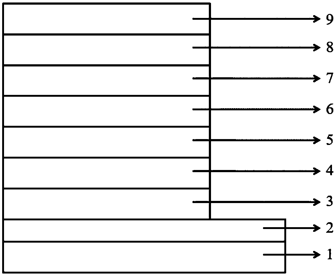
[0072] The structure of the organic electroluminescent device prepared in Example 1 is as follows: figure 2 As shown, the specific preparation process of the device is as follows:
[0073] Clean the ITO anode layer 2 on the transparent glass substrate layer 1, ultrasonically clean it with deionized water, acetone, and ethanol for 15 minutes each, and then treat it in a plasma cleaner for 2 minutes; dry the ITO glass substrate and place it in a vacuum In the cavity, the vacuum degree is less than 2*10 -6 Torr, on the ITO anode layer 2, evaporate 10nm thick HAT-CN, this layer is used as hole injection layer 3; then evaporate 80nm HT1, this layer is used as hole transport layer 4, and then evaporate 20nm thick EB1 , this layer is used as an electron blocking layer 5; further, a luminescent layer 6 of 30nm is evaporated: the selection of the host material and the dopant material are shown in Table 1, and the rate is controlled by a film thickness meter; on the luminescent layer ...
Embodiment 2~60
[0075] Examples 2-60 The methods for preparing organic electroluminescent devices are similar to those of Example 1, and the specific materials used are shown in Table 1.
PUM
 Abstract
Description
Claims
Application Information