Methods of forming a semiconductor structure and methods of forming isolation structures

A silicon material, silicon dioxide technology, applied in semiconductor/solid-state device manufacturing, transistors, electrical components, etc., can solve the problems of reducing active area efficiency, silicon consumption, consumption, etc.

Pending Publication Date: 2019-11-26
MICRON TECH INC
View PDF9 Cites 0 Cited by
  • Summary
  • Abstract
  • Description
  • Claims
  • Application Information

AI Technical Summary

Problems solved by technology

Therefore, the main effect of the process is to consume silicon, reducing the active area efficiency
Metall

Method used


Image

  • Methods of forming a semiconductor structure and methods of forming isolation structures
  • Methods of forming a semiconductor structure and methods of forming isolation structures
  • Methods of forming a semiconductor structure and methods of forming isolation structures

Examples


Embodiment Construction

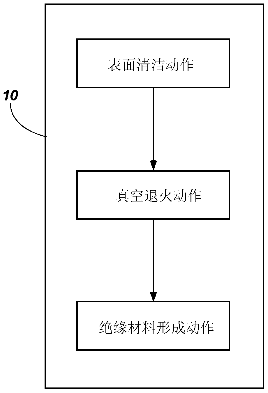
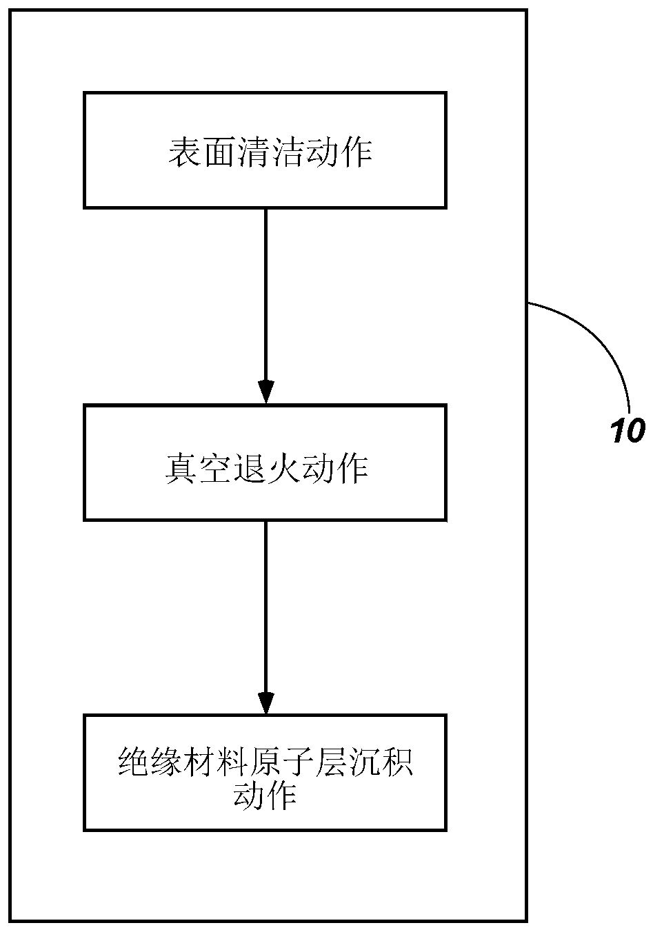
[0016] Methods of forming semiconductor structures comprising silicon material and isolation structures such as shallow trench isolation (STI) structures are disclosed, wherein the semiconductor structures are formed with minimal silicon material consumption (eg, minimal loss). Silicon material is used as the active region where electronic devices will be formed, and a significantly increased amount of silicon material remains after the process actions used to form the semiconductor structure compared to conventional manufacturing techniques. The actions used during fabrication of the semiconductor structure are performed in a manner that minimizes oxidation of the silicon material and repairs damage to the silicon material. Activities include, among other things, cleaning the silicon material, vacuum annealing the silicon material, and forming a high-quality insulating material on the silicon material. High-quality insulating materials have high density, high-quality interfac...


PUM


Abstract

The present invention relates to a method of reducing silicon consumption of a silicon material. The method comprises the steps of: cleaning a silicon material and subjecting the cleaned silicon material to a vacuum anneal at a temperature below a melting point of silicon and under vacuum conditions. The silicon material is subjected to additional process acts without substantially removing silicon of the silicon material. Additional methods of forming a semiconductor structure and forming isolation structures are also disclosed.

Description

[0001] priority claim [0002] This application claims a 2018 application for "Methods for Reducing Silicon Consumption, Methods of Forming a Semiconductor Structure, and Methods of Forming Isolation Structures" The benefit of the filing date of U.S. Patent Application Serial No. 15 / 982,872, filed May 17. technical field [0003] Embodiments disclosed herein relate to semiconductor fabrication, including the fabrication of semiconductor devices, such as dynamic random access memory (DRAM) device fabrication. More particularly, embodiments of the present invention relate to methods of minimizing silicon loss during semiconductor device fabrication, methods of forming semiconductor structures, and methods of forming isolation structures. Background technique [0004] An integrated circuit contains a number of electronic devices, such as transistors or capacitors, in an active area of ​​a substrate. In most cases, the active area comprises silicon, and the various integrated...

Claims


Application Information

Patent Timeline
IPC IPC(8): H01L21/02H01L21/324H01L21/762H01L27/108
CPCH01L21/02057H01L21/324H01L21/76224H10B12/00H01L21/02301H01L21/02164H01L21/0228H01L21/0206
Inventor 古尔特杰·S·桑胡
Owner MICRON TECH INC
Why Eureka
Try Eureka