Inspection jig and inspection method
A fixture and pattern technology, applied in the field of inspection, can solve problems such as inaccurate pixel size, edge collapse or inaccurate processing groove width, and achieve the effect of accurate pixel size
- Summary
- Abstract
- Description
- Claims
- Application Information
AI Technical Summary
Problems solved by technology
Method used
Image


Examples
no. 1 Embodiment approach
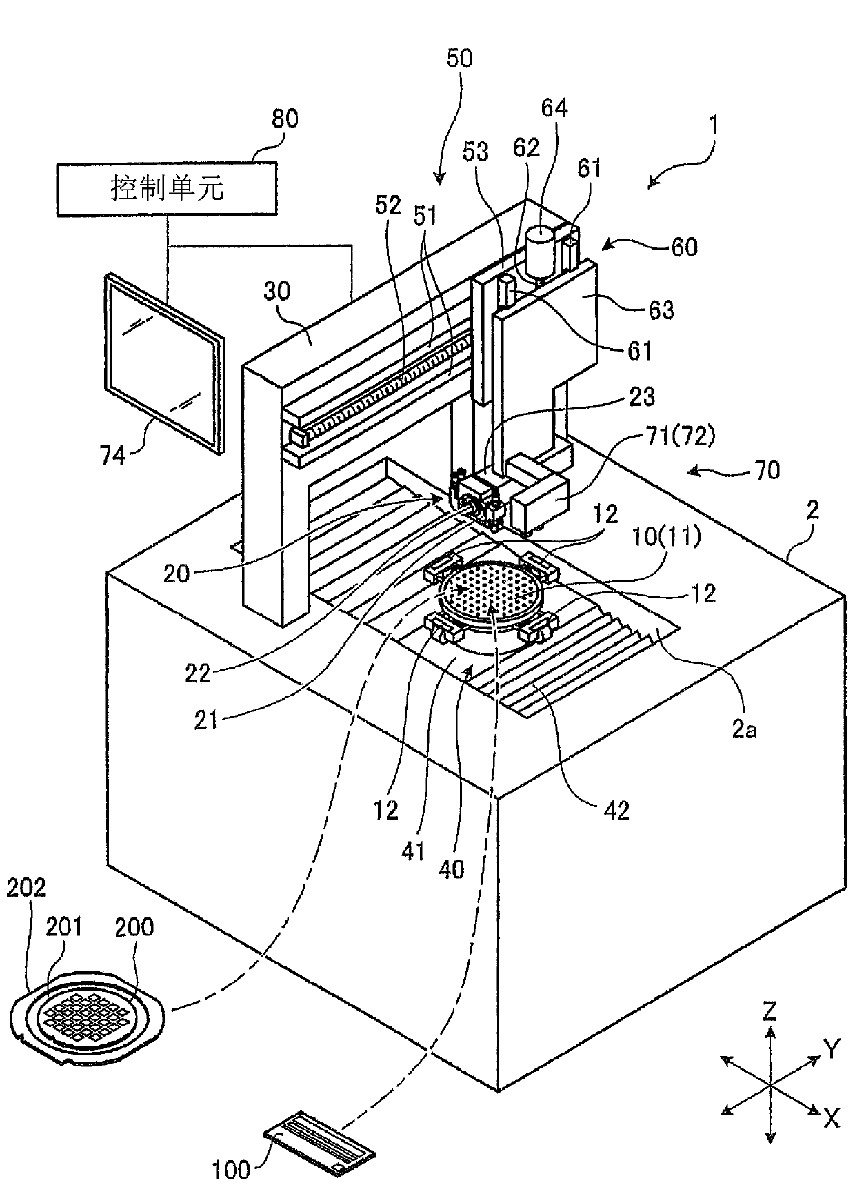
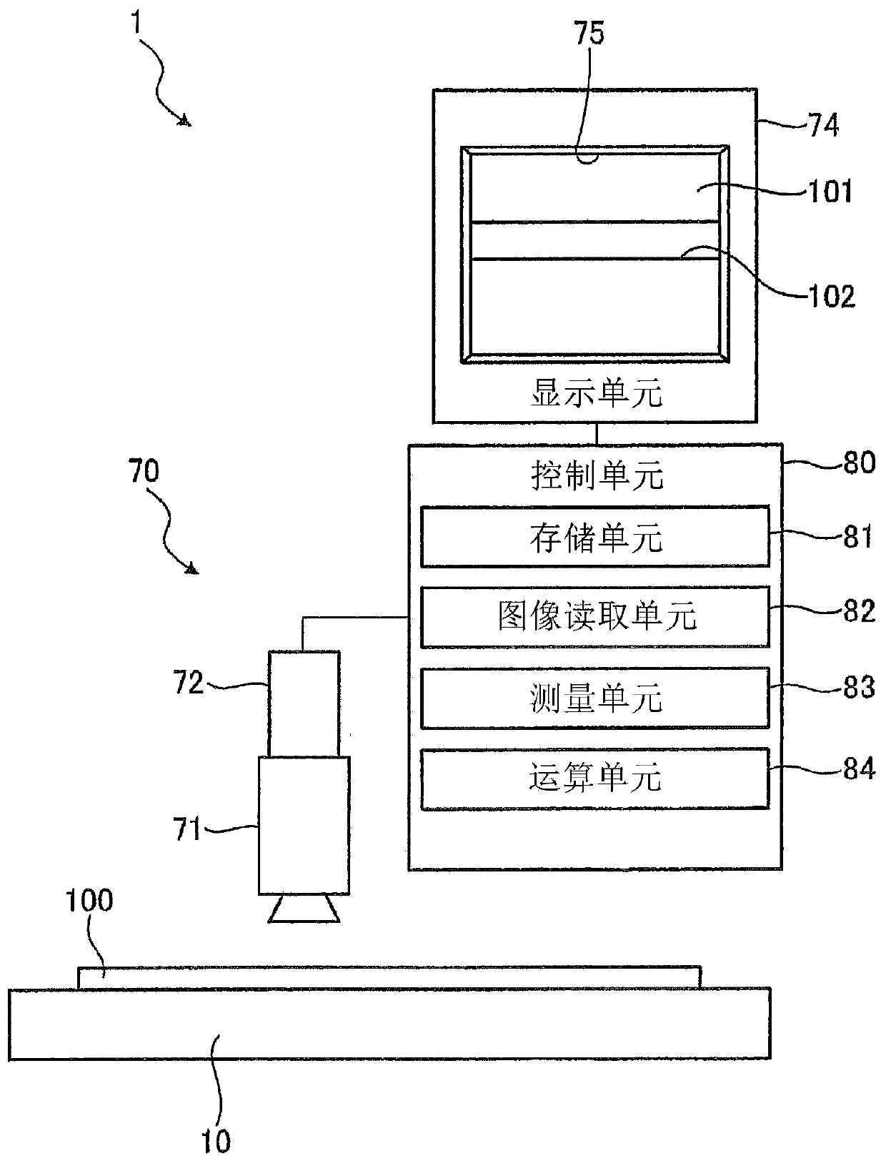
[0022] figure 1 It is a perspective view showing a configuration example of a processing device using the inspection jig of the first embodiment. figure 2 It is a plan view showing a structural example of the inspection jig of the first embodiment. image 3 It is a block diagram showing a configuration example of a control unit of a processing apparatus. The processing apparatus 1 is an apparatus for cutting a wafer 200 as a workpiece to divide the wafer 200 into individual chips. Such as figure 1 As shown, the processing device 1 has a chuck table (holding unit) 10, a processing unit 20, a door frame 30, a processing feed unit 40, an index feed unit 50, a cutting feed unit 60, a photographing unit 70, a display unit 74 and control unit 80.
[0023] The wafer 200 is a workpiece on which semiconductor devices or optical devices are formed, such as semiconductor wafers, optical device wafers, inorganic material substrates, ductile resin material substrates, ceramic substrat...
no. 2 Embodiment approach
[0045] Next, an inspection jig 100A of the second embodiment will be described. Figure 6 It is a plan view showing a configuration example of the inspection jig of the second embodiment. Compared with the inspection jig 100 described above, the inspection jig 100A is different in structure from the inspection jig 100 in that it has a pair of reference patterns 106 and 106 for parallel alignment. The same reference numerals are assigned to the same structures as those of the inspection jig 100 and descriptions thereof are omitted. The pair of reference patterns 106 and 106 are formed in the same shape (cross shape) with the same size. The pair of reference patterns 106 and 106 are arranged side by side in a direction parallel to the longitudinal direction of the first pattern 102 and the like. A pair of reference patterns 106, 106 are cross grooves formed on the front surface of the plate body 101 by etching, cutting or laser processing similarly to the above-mentioned first...
no. 3 Embodiment approach
[0050] Next, an inspection jig 100B according to the third embodiment will be described. Figure 7 It is a plan view showing a configuration example of the inspection jig of the third embodiment. In this third embodiment, an inspection jig 100B has a disc-shaped plate body 101B, and a pair of first reference patterns 107, 107 and a pair of second reference patterns 108, 108 are formed on the front surface of the plate body 101B.
[0051] The plate body 101B is different from the plate body 101 in that it has a disk shape, but the material and the like are the same. The first reference patterns 107 and 107 are formed in the same shape (cross shape) with the same size. The second reference patterns 108, 108 are smaller than the first reference patterns 107, 107, and are formed in the same shape (cross shape) with the same size. The first reference patterns 107, 107 and the second reference patterns 108, 108 are arranged in directions parallel to each other. The first referenc...
PUM
 Abstract
Description
Claims
Application Information
 - R&D
- Intellectual Property
- Life Sciences
- Materials
- Tech Scout
- Unparalleled Data Quality
- Higher Quality Content
- 60% Fewer Hallucinations
Browse by: Latest US Patents, China's latest patents, Technical Efficacy Thesaurus, Application Domain, Technology Topic, Popular Technical Reports.
© 2025 PatSnap. All rights reserved.Legal|Privacy policy|Modern Slavery Act Transparency Statement|Sitemap|About US| Contact US: help@patsnap.com