Bubble defect detection method and system for wafer bonding process
A wafer bonding and defect detection technology, used in electrical components, semiconductor/solid-state device testing/measurement, semiconductor/solid-state device manufacturing, etc. Problems such as reflection signals of bonded wafers, to achieve fast and accurate detection, improve product yield, and avoid batch product abnormalities
- Summary
- Abstract
- Description
- Claims
- Application Information
AI Technical Summary
Problems solved by technology
Method used
Image


Examples
Embodiment Construction
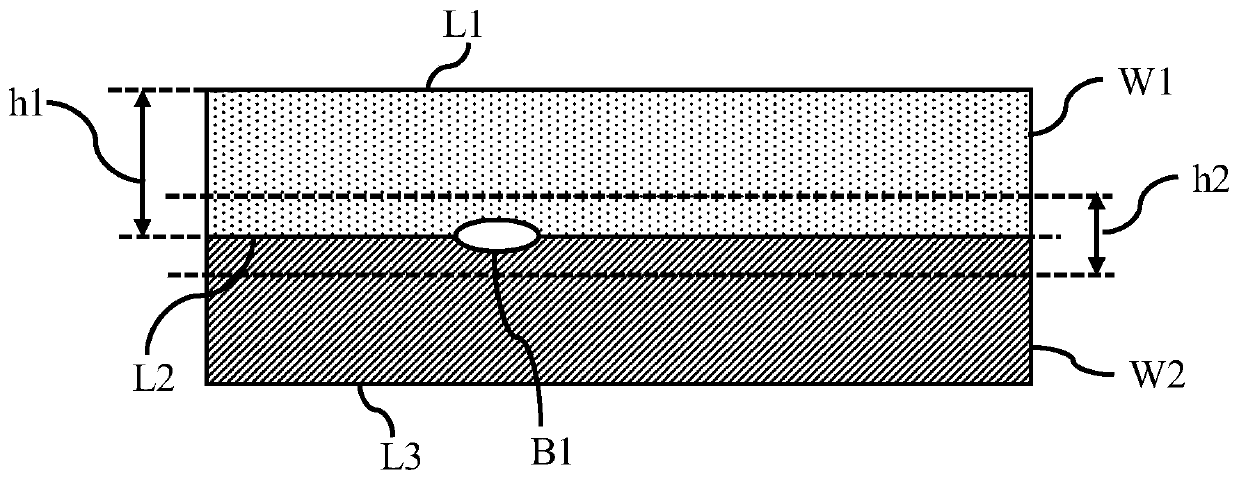
[0034] After research, it is found that the use of ultrasonic testing technology to detect bubbles at the bonding interface of bonded wafers is only applicable before the thinning process. Such as Figure 1aAs shown, after wafer W1 and wafer W2 are bonded, air bubbles may be generated at the bonding interface L2. When the ultrasonic wave reaches the interface between the air and the solid on the bonded wafer, a reflected wave will be formed. The trend of change is reflected in Figure 1b Among them, the X-axis is the time difference from transmitting the ultrasonic wave to receiving the reflected wave, and the Y-axis is the signal strength of the reflected wave. When the ultrasonic wave reaches the upper surface L1 of the wafer W1, a reflected wave N1 is formed; when the ultrasonic wave reaches the bonding interface L2 between the wafer W1 and the wafer W2, if there is a bubble B1 at the bonding interface L2, it will appear in the signal window H2 A reflected wave appears in ...
PUM
| Property | Measurement | Unit |
|---|---|---|
| Thickness | aaaaa | aaaaa |
Abstract
Description
Claims
Application Information
 - R&D
- Intellectual Property
- Life Sciences
- Materials
- Tech Scout
- Unparalleled Data Quality
- Higher Quality Content
- 60% Fewer Hallucinations
Browse by: Latest US Patents, China's latest patents, Technical Efficacy Thesaurus, Application Domain, Technology Topic, Popular Technical Reports.
© 2025 PatSnap. All rights reserved.Legal|Privacy policy|Modern Slavery Act Transparency Statement|Sitemap|About US| Contact US: help@patsnap.com