GaN-based PIN diode device structure and preparation method thereof

A PIN diode and device structure technology, which is applied in the field of new PIN diode device structure, can solve the problems of crystal quality degradation, leakage current increase, N-doping overweight, etc., achieve uniform current expansion, ease current congestion, and simple and reliable process Effect

Pending Publication Date: 2019-12-06
HEBEI UNIV OF TECH
View PDF13 Cites 2 Cited by
  • Summary
  • Abstract
  • Description
  • Claims
  • Application Information

AI Technical Summary

Problems solved by technology

In this type of structure, after exposing n-type GaN by means of mesa etching, p-type ohmic electrodes and n-type ohmic electrodes are prepared on the surface of p-GaN layer and n-GaN layer, a major disadvantage of this design It is in the forward working area of ​​the device, the current is crowded at the edge of the table, so the Auger recombination effect is more obvious
In order to slow down the crowding effect of the current at the edge of the mesa, one of the ways is to increase the doping concentration or increase the thickness of the N-type heavily doped semiconductor electron transport layer, thereby reducing the resistance of the layer and slowing down the edge crowding effect of the current ( Zhang, et al. "Reduction of on-Resistance and Current Crowding in Quasi-Vertical GaN Power Diodes." Applied Physics Letters 111,16(2017):163506.), but this way N doping is too heavy, will be in the crystal A large number of defects are introduced into the lattice, the quality of the crystal decreases, and the leakage current increases

Method used


Image

  • GaN-based PIN diode device structure and preparation method thereof
  • GaN-based PIN diode device structure and preparation method thereof
  • GaN-based PIN diode device structure and preparation method thereof

Examples


Embodiment 1

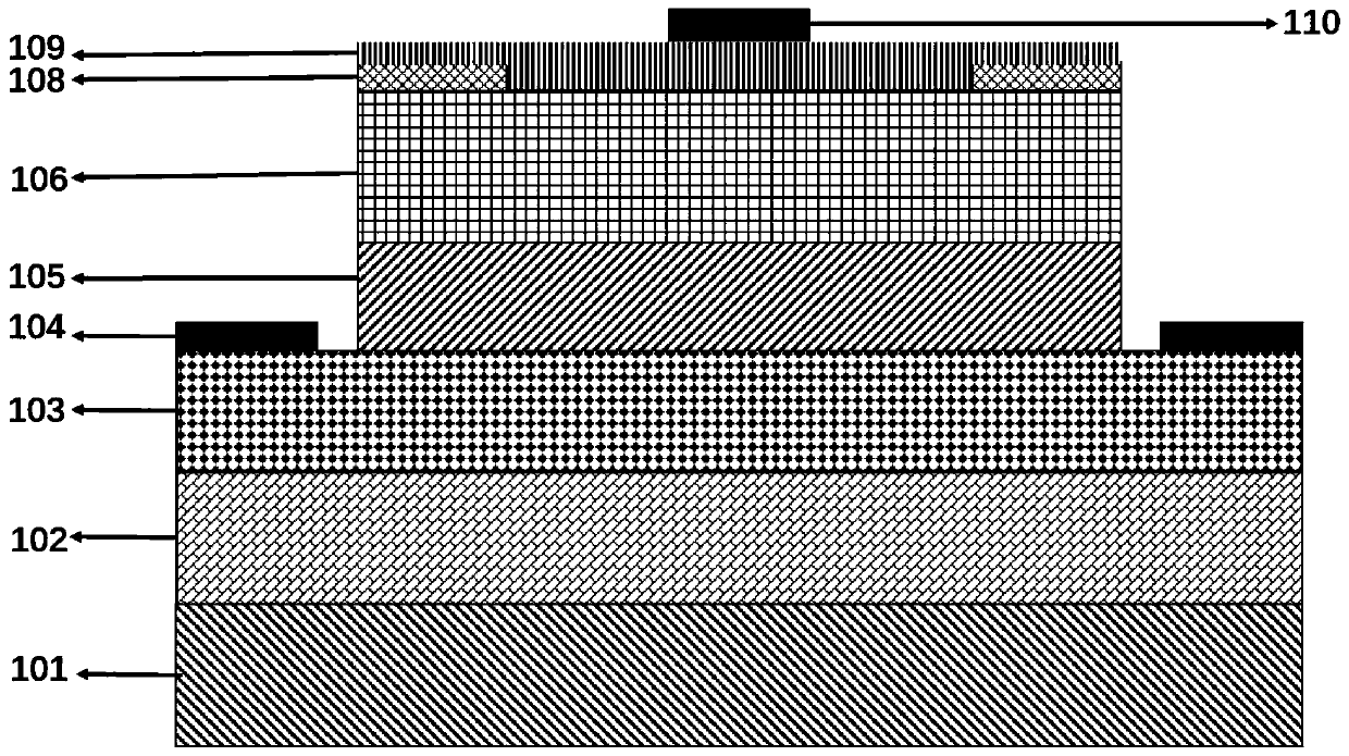
[0067] This embodiment has a PIN diode device structure (the device in this embodiment is cylindrical), and the diode device structure includes in sequence along the epitaxial growth direction: a substrate 101, a buffer layer 102, and an N-type heavily doped semiconductor transport layer 103;

[0068] An N-type intrinsic layer 105 is distributed on the N-type heavily doped semiconductor transport layer 103, the two centers are the same, and the projected area of ​​the N-type intrinsic layer 105 is N-type heavily doped semiconductor transport layer 103 50% of;

[0069] A P-type heavily doped semiconductor transport layer 106 is grown on the N-type intrinsic layer 105, and the top outer ring portion of the P-type heavily doped semiconductor transport layer 106 is an N-type insertion layer 107. The projected area of ​​the N-type insertion layer 107 is 50% of the area of ​​the P-type heavily doped semiconductor transport layer 106;

[0070] The N-type insertion layer 107 is obta...

Embodiment 2

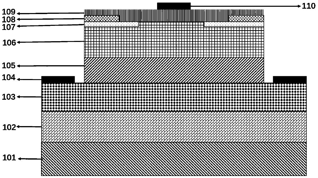
[0089] This embodiment has a vertical PIN diode device structure, which sequentially includes along the epitaxial growth direction: an N-type heavily doped semiconductor transport layer 103; the N-type heavily doped semiconductor transport layer 103 is distributed There is an N-type intrinsic layer 105; a P-type heavily doped semiconductor transport layer 106 is grown on the N-type intrinsic layer 105, and the ring-shaped portion at the top of the P-type heavily doped semiconductor transport layer 106 is N-type insertion layer 107; the N-type insertion layer 107 is obtained by implanting N-type ions into the material of the P-type heavily doped semiconductor transport layer 106, the N-type ions are silicon ions, and the implanted Quantity is 10 18 cm -3 . A ring-shaped insulating layer 108 is grown on the outer edge of the N-type insertion layer 107; the current spreading layer 109 is formed on the insulating layer 108 and the exposed P-type heavily doped semiconductor trans...


PUM

PropertyMeasurementUnit
Thicknessaaaaaaaaaa
Thicknessaaaaaaaaaa
Thicknessaaaaaaaaaa

Abstract

The invention relates to a GaN-based PIN diode device structure and a preparation method thereof. The diode device structure sequentially comprises a substrate, a buffer layer and an N-type heavily-doped semiconductor transmission layer in the epitaxial growth direction, wherein an N-type intrinsic layer is distributed on the N-type heavily-doped semiconductor transmission layer, a P-type heavily-doped semiconductor transmission layer grows on the N-type intrinsic layer, the annular part of the outer edge of the top of the P-type heavily-doped semiconductor transmission layer is an N-type insertion layer, and the N-type insertion layer is obtained by injecting N-type ions into the material of the P-type heavily-doped semiconductor transmission layer; an annular insulating layer grows on the outer edge of the N-type insertion layer; and then the current expansion layer and the P-type ohmic electrode are sequentially arranged, and an N-type ohmic electrode is located on the exposed N-type heavily-doped semiconductor transmission layer. According to the invention, the concentration of edge carriers is effectively reduced, more uniform current expansion is realized, and the reverse breakdown voltage is not influenced.

Description

technical field [0001] The invention relates to the technical field of power electronic devices, in particular to a novel PIN diode device structure which reduces the edge carrier concentration, suppresses Auger recombination and slows down the current crowding effect. Background technique [0002] PIN diodes are mainly composed of heavily doped n+ type and p+ type semiconductor transmission layers, sandwiching an intrinsic layer (I layer) with high resistivity, so as to achieve a high reverse breakdown voltage and achieve a certain Signal modulation capabilities in the frequency range. The PIN diode is based on the PN junction structure, through the injection of minority carriers (referred to as minority), to realize the forward open-state working process, this process is called conductance modulation, and the drift region is compared by conductance modulation during forward conduction Small on-resistance, so that the device can use the low-doped drift region to obtain a h...

Claims


Application Information

Patent Timeline
IPC IPC(8): H01L29/06H01L29/868H01L21/329
CPCH01L29/868H01L29/6609H01L29/0684
Inventor 张紫辉刘亚津张勇辉贾兴宇
Owner HEBEI UNIV OF TECH
Why Eureka
Try Eureka