Unlock instant, AI-driven research and patent intelligence for your innovation.

Microswitch array module

A micro-switch and array technology, applied in the field of micro-switches, can solve the problems of increased manufacturing cost, complex structure, low yield and the like, and achieve the effects of low manufacturing cost, low manufacturing cost and simple process.

Active Publication Date: 2019-12-10
TRIPLE POWER LTD
View PDF5 Cites 0 Cited by
  • Summary
  • Abstract
  • Description
  • Claims
  • Application Information

AI Technical Summary

Problems solved by technology

That is to say, in the current cholesteric liquid crystal writing tablet with position detection function, the structure of the element responsible for position sensing is relatively complicated, so the manufacturing cost is relatively increased
Also, because of the additional semiconductor process steps, the yield rate is low

Method used


Image

  • Microswitch array module
  • Microswitch array module
  • Microswitch array module

Examples


no. 1 example

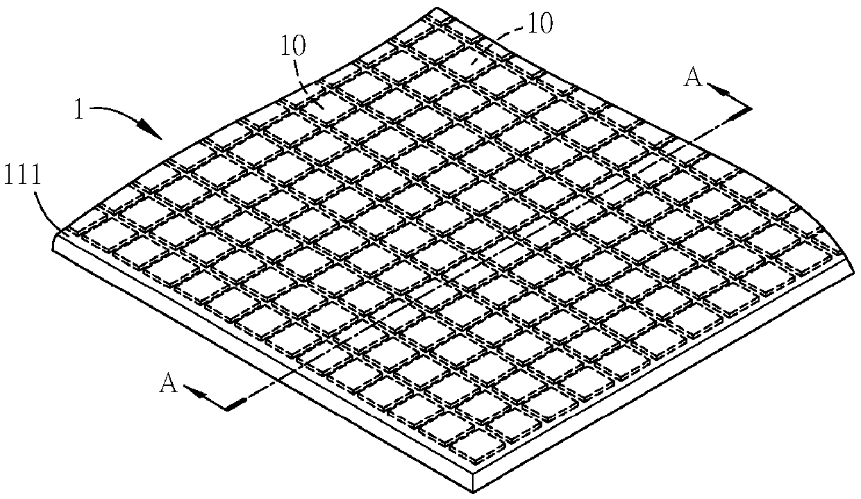
[0023] figure 1 It is a three-dimensional schematic diagram of a micro switch array module according to an embodiment of the present invention. Figure 2A for figure 1 The shown schematic diagram of the structure of the micro switch array module along the A-A section line.

[0024] Such as figure 1 and Figure 2A As shown, the micro switch array module 1 has a plurality of micro switch units 10 arranged in an array. The micro switch unit 10 of this embodiment is configured in a two-dimensional array as an example. Each micro switch unit 10 includes a first transparent substrate 11, a second transparent substrate 13, a transparent conductive layer 12, a first transparent electrode layer 14 and at least one spacer 15.

[0025] The first transparent substrate 11 has a light incident surface 111. The light incident surface 111 of this embodiment is the upper surface of the first transparent substrate 11, and is also the surface of the microswitch array module 1 facing the user, which ...

no. 2 example

[0042] In addition, please refer to Figure 3A and Figure 3B , Which are respectively structural schematic diagrams of a micro switch array module according to another embodiment of the present invention, and Figure 3A The illustrated schematic diagram of the structure of the micro switch electronic writing board composed of the micro switch array module and the cholesterol liquid crystal module.

[0043] The micro switch array module 1 of this embodiment is substantially the same as the micro switch array module described in the previous embodiment. The main difference is that such as Figure 3A As shown, in the micro switch array module 1 of this embodiment, the first transparent electrode layer 14 is disposed on the first surface 131 of the second transparent substrate 13, and extends to the second transparent electrode layer through the first conductive hole 133. On the second surface 132 of the optical substrate 13, corresponding and spaced first transparent electrode laye...


PUM

PropertyMeasurementUnit
Thicknessaaaaaaaaaa

Abstract

The invention provides a micro-switch array module. The micro-switch array module is provided with a plurality of micro-switch units. Each microswitch unit comprises a first light-transmitting substrate, a transparent conductive layer, a second light-transmitting substrate, a first transparent electrode layer and at least one spacer. The first light-transmitting substrate has a light incident surface. The transparent conductive layer is arranged on the surface, opposite to the light incident surface, of the first light-transmitting substrate. The second light-transmitting substrate is providedwith a first surface facing the transparent conductive layer and a second surface opposite to the first surface, wherein the second light-transmitting substrate is provided with a first conductive hole penetrating through the first surface and the second surface. The first transparent electrode layer is arranged on the first surface of the second light-transmitting substrate and extends into thefirst conductive hole. The spacer is arranged between the first light-transmitting substrate and the second light-transmitting substrate.

Description

Technical field [0001] The invention relates to a micro switch, in particular to a micro switch module arranged in an array. Background technique [0002] Cholesteric liquid crystal is the addition of a chiral dopant to nematic liquid crystal to make it have a spiral arrangement structure, and use two different liquid crystal molecular arrangements that reflect and penetrate under different voltage differences. State to achieve different light penetration rates to achieve display effects. Among them, in the planar state, the incident light will be reflected and colored; in the focal conic state, most of the incident light will penetrate and a small part of it will be scattered; and in the vertical state, the incident light will completely penetrate. [0003] Since the cholesteric liquid crystal is in a stable state when it is in the planar state and the focal conic state, when the voltage is turned off and disappears, it will still maintain the original state and display screen. I...

Claims


Application Information

Patent Timeline
IPC IPC(8): G02F1/1343G02F1/1333G02F1/137
CPCG02F1/134309G02F1/13439G02F1/1333G02F1/13718
Inventor 王富民
Owner TRIPLE POWER LTD
Features
  • R&D
  • Intellectual Property
  • Life Sciences
  • Materials
  • Tech Scout
  • Unparalleled Data Quality
  • Higher Quality Content
  • 60% Fewer Hallucinations
Learn More