LED chip and manufacturing method thereof

A technology of LED chips and gallium nitride layers, which is applied in the direction of electrical components, circuits, semiconductor devices, etc., can solve the problems that the brightness of LED chips needs to be improved, and achieve the effects of improving light utilization, increasing current, and good ohmic contact performance

Active Publication Date: 2019-12-13
XIAMEN CHANGELIGHT CO LTD
View PDF4 Cites 1 Cited by
  • Summary
  • Abstract
  • Description
  • Claims
  • Application Information

AI Technical Summary

Problems solved by technology

However, the brightness of existing LED chips needs to be improved

Method used


Image

  • LED chip and manufacturing method thereof
  • LED chip and manufacturing method thereof
  • LED chip and manufacturing method thereof

Examples


Embodiment Construction

[0051]The following will clearly and completely describe the technical solutions in the embodiments of the application with reference to the drawings in the embodiments of the application. Apparently, the described embodiments are only some of the embodiments of the application, not all of them. Based on the embodiments in this application, all other embodiments obtained by persons of ordinary skill in the art without making creative efforts belong to the scope of protection of this application.

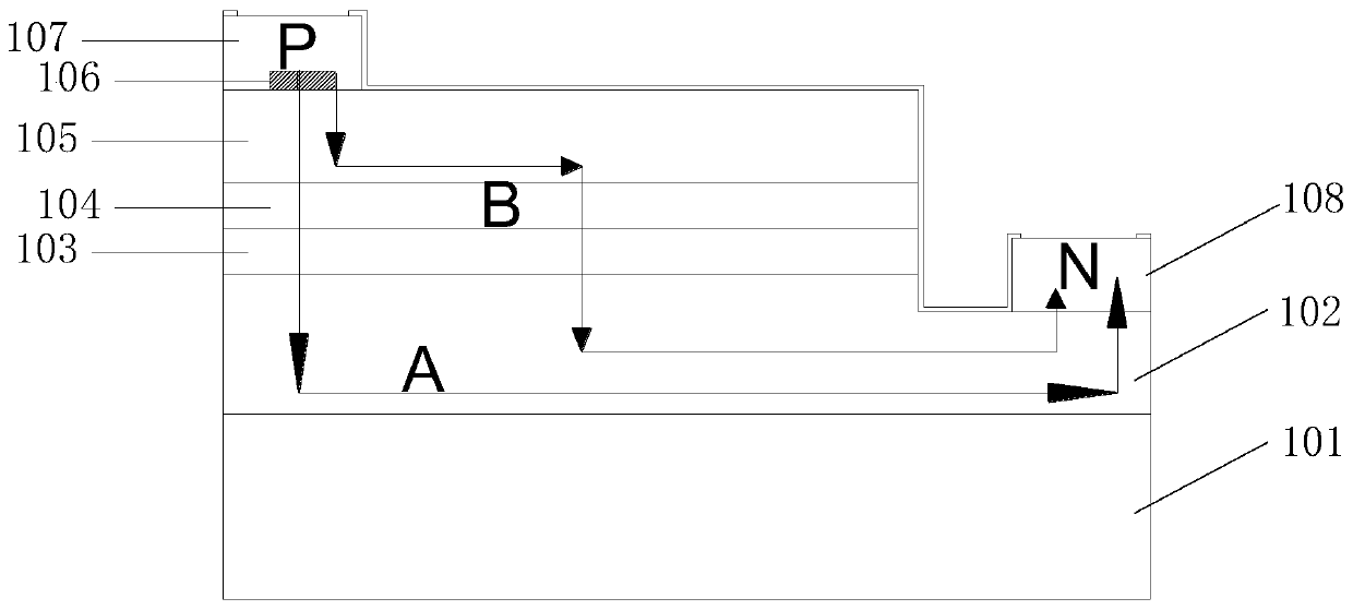
[0052] As mentioned in the background art, the brightness of existing LED chips needs to be improved.

[0053] Such as figure 1 As shown, the existing LED chip includes from bottom to top: a substrate 101, an N-type GaN layer 102, an active layer 103, a P-type GaN layer 104, a current spreading layer 105 electrically connected to the P-type GaN layer, and a The current blocking layer 106 on the surface of the current spreading layer 105 , the P electrode 107 covering the current blo...


PUM

PropertyMeasurementUnit
thicknessaaaaaaaaaa
thicknessaaaaaaaaaa
thicknessaaaaaaaaaa

Abstract

The embodiment of the invention provides an LED chip and a manufacturing method thereof. The LED chip comprises a substrate, an epitaxial structure, a current blocking layer, a composite film layer, afirst electrode and a second electrode, wherein the epitaxial structure is located on the first surface of the substrate and comprises a first gallium nitride layer, an active layer and a second gallium nitride layer, and the first gallium nitride layer and the second gallium nitride layer are different in doping type; the current blocking layer is located in a preset region on the side, which isaway from the substrate, of the second gallium nitride layer; the composite film layer is located on the side, which is away from the second gallium nitride layer, of the current blocking layer and covers the second gallium nitride layer, the composite film layer comprises an ohmic contact layer, an insulating dot matrix layer and a first conducting layer which are laminated, and the insulating dot matrix layer comprises a plurality of discontinuous insulating units; the first electrode is electrically connected with the side, which is away from the substrate, of the first gallium nitride layer; and the second electrode is electrically connected with the side, which is away from the second gallium nitride layer, of the composite film layer. The LED chip has relatively high current transverse expansion capability and relatively high light-emitting brightness.

Description

technical field [0001] The present application relates to the field of semiconductor light emitting devices, in particular to an LED chip and a manufacturing method thereof. Background technique [0002] With the rapid development of LED technology and the gradual improvement of LED light efficiency, the application of LED is becoming more and more extensive, and people are paying more and more attention to the development prospect of LED in the lighting market. LED chip, as the core component of LED lamp, its function is to convert electrical energy into light energy. Specifically, the LED chip includes a P-type semiconductor layer, an N-type semiconductor layer, and a When the current passes through the LED chip, the holes in the P-type semiconductor and the electrons in the N-type semiconductor will move to the active layer and recombine in the active layer, making the LED chip emit light. However, the brightness of the existing LED chips needs to be improved. Contents...

Claims


Application Information

Patent Timeline
Patent Type & Authority Applications(China)
IPC IPC(8): H01L33/14H01L33/42H01L33/00
CPCH01L33/007H01L33/14H01L33/145H01L33/42
Inventor 刘伟李俊贤刘英策蔡和勋邬新根
Owner XIAMEN CHANGELIGHT CO LTD
Why Eureka
Try Eureka