
Photonic frequency up-conversion device and growth method thereof

A growth method and frequency technology, applied in the field of photon frequency up-conversion devices and their growth, can solve the problems of limiting the application of up-conversion devices, high cost, cumbersome preparation process, etc., and achieve low-cost large-scale preparation, compact structure, and high-quality devices Effect of Up-Conversion Efficiency Improvement

Inactive Publication Date: 2019-12-17
SHANGHAI JIAO TONG UNIV
View PDF5 Cites 0 Cited by
  • Summary
  • Abstract
  • Description
  • Claims
  • Application Information

AI Technical Summary

Problems solved by technology

However, this technology requires epitaxial growth of light-emitting diodes and infrared detectors twice, and then integrated together by wafer bonding.
The high cost of double epitaxial growth and wafer bonding and the cumbersome preparation process greatly limit the application of this up-conversion device

Method used


Image

  • Photonic frequency up-conversion device and growth method thereof
  • Photonic frequency up-conversion device and growth method thereof
  • Photonic frequency up-conversion device and growth method thereof

Examples


Embodiment 1

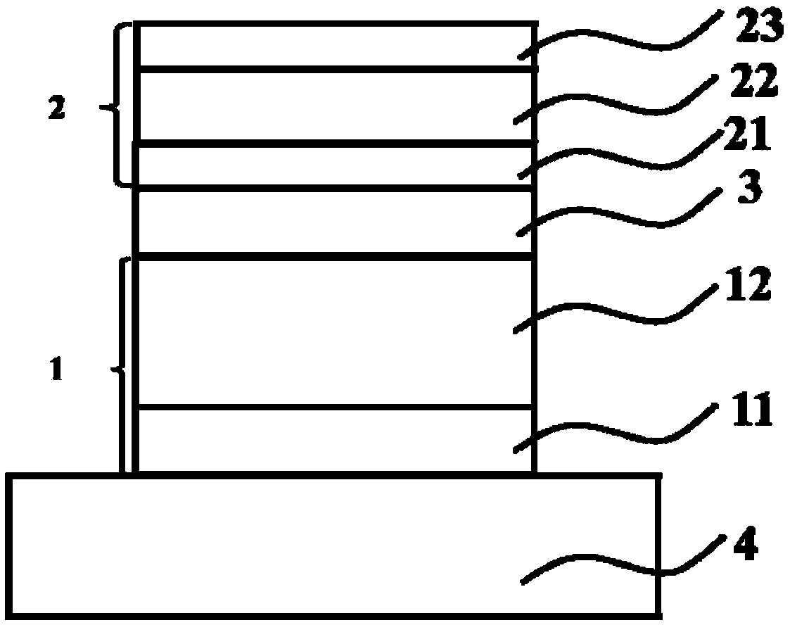
[0117] A photonic frequency upconversion device grown by direct epitaxial growth, such as Figure 8 As shown, it is a near-infrared photon frequency up-conversion device for direct epitaxial growth of the present invention, including three parts: a near-infrared detector 1, a graded layer 3 and a light-emitting diode 2; wherein the near-infrared detector 1 absorbs the incident near-infrared light signal, It is converted into photo-generated carriers, and the generated photo-generated carriers will migrate to the active region of the light-emitting diode 2 under the action of an electric field for radiative recombination to emit short-wave near-infrared photons or visible photons, thereby realizing up-conversion. During growth, the near-infrared photon frequency up-conversion device is obtained by direct epitaxial growth on a substrate with a thickness of 500 μm and a substrate layer 4 of InP by MBE method. During epitaxy, the near-infrared detector 1 is epitaxially grown on th...

Embodiment 2

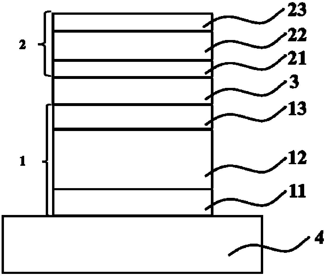
[0122] A photonic frequency upconversion device grown by direct epitaxial growth, such as Figure 9 As shown, it is a near-infrared photon frequency up-conversion device for direct epitaxial growth of the present invention. During growth, the near-infrared photon frequency up-conversion device is directly epitaxially grown on a substrate with a thickness of 700um and a substrate layer 4 of InP by MOCVD method get. During epitaxy, the near-infrared detector 1 is epitaxially grown on the InP first, then the gradient layer is epitaxially grown on the p-type InP of the near-infrared detector 1 , and finally the light-emitting diode 2 is epitaxially grown on the gradient layer 3 .

[0123] The near-infrared detector 1 is InP / In containing a P-type cap layer 13 0.53 Ga 0.47 As p-i-n infrared detector: the n-type cap layer 11 is n-type InP with a thickness of 400nm; the intrinsic absorption layer 12 is InGaAs with a thickness of 2μm, and the p-type cap layer 13 is p-type InP with a...

Embodiment 3

[0127] A photonic frequency upconversion device grown by direct epitaxial growth, such as Figure 10 As shown, it is a near-infrared photon frequency up-conversion device grown by direct epitaxial growth in the present invention, which includes a near-infrared detector 1 , a graded layer 3 and a light-emitting diode 2 . During growth, the near-infrared photon frequency up-conversion device is obtained by direct epitaxial growth on a substrate with a thickness of 600 um and a substrate layer 4 of InP by CVD. During epitaxy, the near-infrared detector 1 is epitaxially grown on InP first, then the gradient layer 3 is epitaxially grown on the intrinsic absorption layer 12 of the near-infrared detector 1 , and finally the light-emitting diode 2 is epitaxially grown on the gradient layer 3 .

[0128] The near-infrared detector 1 is an InP / InGaAs n-i infrared detector without a p-type cap layer: the n-type cap layer 11 is n-type InP with a thickness of 600 nm; the intrinsic absorptio...


PUM

PropertyMeasurementUnit
Luminous wavelengthaaaaaaaaaa
Thicknessaaaaaaaaaa
Thicknessaaaaaaaaaa

Abstract

The invention provides a novel photonic frequency up-conversion device and a method. The device comprises a near-infrared photoelectric detector (1), a light emitting diode (2) and a gradient layer (3), wherein the gradient layer (3) is located between the near-infrared photoelectric detector (1) and the light emitting diode (2); and the gradient layer (3) is used for overcoming the influence of lattice mismatch between the near-infrared photoelectric detector (1) and the light emitting diode (2). According to the method, the whole photonic frequency double-conversion device can be obtained through one-time direct field growth, and a wafer bonding step is not needed, so that the photonic up-conversion device is compact in structure, the preparation process is greatly simplified, the cost is reduced, and the up-conversion efficiency is improved.

Description

technical field [0001] The invention relates to the field of semiconductor devices, in particular to a direct epitaxial growth photon frequency up-conversion device and a growth method thereof. Background technique [0002] Infrared up-conversion technology refers to a technical method that converts infrared light signals into short-wave infrared or visible light signals for detection. It has a wide range of applications in laser cooling, material quality inspection, pixel-free imaging, and single-photon detection. In the past decades, various upconversion technologies have been invented, including thermally excited infrared upconversion, rare earth ion infrared upconversion, optical parametric infrared upconversion, Auger infrared upconversion, two-step-two-photon absorption infrared upconversion , infrared detector-light-emitting diode (PD-LED) infrared up-conversion, etc. Among them, optical parametric up-conversion technology is currently the main up-conversion technolo...

Claims


Application Information

Patent Timeline
IPC IPC(8): H01L25/16H01L31/0304H01L31/101H01L31/18H01L33/00H01L33/30
CPCH01L25/167H01L31/0304H01L31/101H01L31/184H01L33/0062H01L33/30Y02P70/50
Inventor 张月蘅白鹏
Owner SHANGHAI JIAO TONG UNIV
Learn More