Supercharge Your Innovation With Domain-Expert AI Agents!

Method for improving silk-screen welding-resistant efficiency of circuit board

A technology of silk screen and solder mask, applied in the field of improving the efficiency of screen printing and solder mask of circuit boards, can solve problems such as hidden dangers, copper surface prone to oxidation quality, low efficiency, etc., and achieve the effect of improving production efficiency and saving pre-baking time.

Active Publication Date: 2019-12-20
JIANGMEN SUNTAK CIRCUIT TECH
View PDF10 Cites 3 Cited by
  • Summary
  • Abstract
  • Description
  • Claims
  • Application Information

AI Technical Summary

Problems solved by technology

[0003] The present invention aims at the problem that the current silk screen solder resist method for double-sided circuit boards needs to carry out two standing and pre-baking processes, the efficiency is low, and the copper surface on the side that has not yet been silk screen solder resist ink is prone to oxidation and leads to quality problems. It provides A method that can improve the efficiency of silk screen solder masking of circuit boards by only one static and pre-baking treatment

Method used


Image

  • Method for improving silk-screen welding-resistant efficiency of circuit board
  • Method for improving silk-screen welding-resistant efficiency of circuit board
  • Method for improving silk-screen welding-resistant efficiency of circuit board

Examples


Embodiment

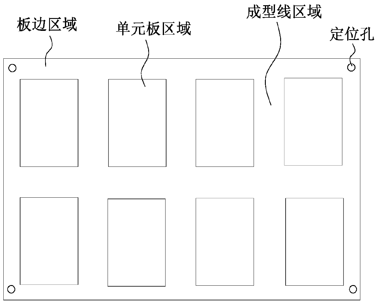
[0027] This embodiment provides a method for improving the efficiency of silk screen solder masking of circuit boards. The PCB production boards of silk screen solder masking are as follows: figure 1 As shown, the PCB production board is divided into the following areas: the board edge area, the unit board area, and the forming line area isolating each unit board area; positioning holes are provided on the board edge area at the four corners of the PCB production board.

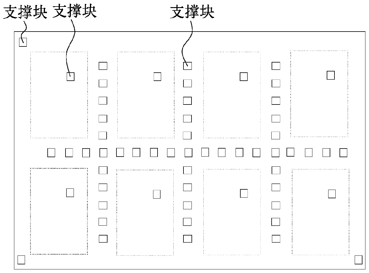
[0028] According to the size of the PCB production board and its area division, the silk screen auxiliary board is made, and the silk screen auxiliary board is 20mm larger than the single side of the PCB production board. The silk screen auxiliary board is divided into areas corresponding to the board edge area, the unit board area and the forming line area of ​​the PCB production board, and the support is set on the board edge area at the triangle of the silk screen auxiliary board and at the position corresp...


PUM


Abstract

The invention relates to the technical field of a printed circuit board, in particular to a method for improving silk-screen welding-resistant efficiency of a circuit board. A silk-screen auxiliary plate with a support block is used in a matching way when welding-resistant ink is silk-screened on a second surface of a PCB production plate, silk-screen can be immediately performed on the second surface after the welding-resistant ink is silk-screened on a first surface, silk-screen of the second surface can be performed without standing and waiting for the welding-resistant ink on the first surface to be dried and pre-baking, the time of first-time standing and pre-baking can be saved, the production efficiency is improved, and the situation that a copper surface on the second surface is exposed in humid and warn air to cause oxidization and introduce a quality potential risk also can be prevented; and meanwhile, the influence factors of pre-baking on the welding-resistant ink on the two surfaces also can be consistent, control of a subsequent developing process is facilitated, and a welding-resistant layer with higher accuracy is developed.

Description

technical field [0001] The invention relates to the technical field of printed circuit boards, in particular to a method for improving the efficiency of silk screen soldering resistance of circuit boards. Background technique [0002] In the field of circuit board production, circuit board solder mask refers to the coating of solder resist ink on the circuit and substrate that does not need to be welded on the board surface to form a protective layer that prevents bridging between circuits during soldering, and serves as a permanent It is a protective layer for the permanent electrical environment and chemical corrosion resistance, and the solder mask of the circuit board also plays a role in beautifying the appearance. Soldering of circuit boards is generally done by screen printing followed by alignment exposure and development, so it is also called silk screen soldering. In addition to traditional single-sided boards, double-sided boards and multi-layer boards require si...

Claims


Application Information

Patent Timeline
IPC IPC(8): H05K3/28
CPCH05K3/282
Inventor 寻瑞平戴勇杨勇汪广明
Owner JIANGMEN SUNTAK CIRCUIT TECH
Features
  • R&D
  • Intellectual Property
  • Life Sciences
  • Materials
  • Tech Scout
  • Unparalleled Data Quality
  • Higher Quality Content
  • 60% Fewer Hallucinations
Learn More