[0047] The specific implementation manner of the present invention will be described below in conjunction with the accompanying drawings.
[0048] In the following description, many specific details are set forth in order to fully understand the present invention, but the present invention can also be implemented in other ways different from those described here, therefore, the present invention is not limited to the specific embodiments disclosed below limit.
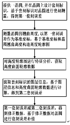
[0049]In order to solve the overlay error caused by the height difference caused by wafer deformation and warpage, the present invention provides an overlay error compensation method and system for a three-dimensional device. On the basis of the existing overlay measuring method, the invention adds the correction and compensation of wafer warpage height and layer thickness to overlay error. That is, on the basis of measuring the first set of engraving errors between wafer overlay marks, then measure the warpage height of the wafer, take the first set of engraving errors as the reference coordinates, and construct the height based on the reference coordinates and wafer warpage height Contour map; use data denoising and fitting algorithm to analyze the characteristics of the height profile map to obtain the height surface profile data; calculate the warpage caused by wafer warpage based on the wafer height surface profile data and the layer information of the overlay mark The second engraving error; the first engraving error minus the second engraving error to obtain the correction data, based on the correction data, the wafer is compensated for the overlay error, and the overlay error measured by the traditional overlay measurement method is compensated. Overlay errors due to height differences due to wafer deformation and warpage are resolved. The invention eliminates the random error caused by measuring the warpage height of the wafer through the data denoising and fitting algorithm, and restores the influence of the warpage height of the wafer on the overlay measurement to the greatest extent. At the same time, the present invention improves the existing overlay measurement system. In the existing overlay measurement system, by adding a laser ranging unit, the warpage height of the wafer can be accurately measured and converted into the error correction coefficient to realize Corrections and performance improvements to existing overlay measurement systems.
[0050] An embodiment of an overlay error compensation method for a three-dimensional device provided by the present invention, see for details Figure 1-Figure 3 , Figure 4a-Figure 4d , Figure 5a-5c and Figure 6a-Figure 6c , the method includes:
[0051] S101: Provide a wafer 4, design an overlay mark on the wafer 4, perform overlay measurement on the wafer 4 based on the overlay mark, and obtain a first overlay error.
[0052] It should be noted that the wafer 4 selected in this step is a warped wafer. The wafer 4 includes the current layer and the front layer relative to the current layer. Both the current layer and the front layer of the wafer 4 are designed with overlay marks. Overlay measurement on wafer 4 based on current layer overlay 1 and previous layer overlay 2 (see figure 2 ), the measurement of the first overlay error here does not consider the overlay error caused by the deformation or warpage of the wafer 4 .
[0053] Overlay measurement methods, including image-based overlay measurement or diffraction-based overlay measurement.
[0054] For image-based overlay measurement, its overlay marks include Box-in-box, Bar-in-bar and AIM and other commonly used overlay marks in integrated circuits. The optical image information is used to calculate the center coordinates of the overlay marks of the two layers, and thus obtain the position deviation of the center coordinates, which is the first overlay error.
[0055] For the overlay measurement based on diffraction, the overlay mark is an equiperiod grating stripe structure, and the first overlay error is calculated by measuring the intensity difference between the positive and negative first-order diffracted light passing through the equiperiod grating of the current layer and the previous layer.
[0056] Preferably, the first overlay error is obtained using a diffraction based overlay measurement.
[0057] Further, wafer overlay marking and layer structure (see figure 2 ) size and period can be appropriately adjusted according to the demand. With the continuous reduction of integrated circuit computing nodes, the wafer overlay mark and layer structure (see figure 2 ) size and period are also constantly adjusted, for example, the size of the AIM structure proposed by KLA company is gradually reduced from 24 microns × 24 microns to 10 microns × 10 microns, or even smaller, to meet the ever-increasing overlay requirements; based on diffraction The period of the equal-period grating stripe structure of the overlay mark may be adjusted with the specific process and detection wavelength; in addition, for the self-aligned imaging process, a fine structure with a nanometer width needs to be added to the overlay mark. The width of the engraved logo needs to be optimized or fine-tuned according to the simulation situation.
[0058] S102: Measure the warpage height of the wafer 4, use the first engraving error as a reference coordinate, and construct a height profile map based on the reference coordinate and the warpage height of the wafer 4.
[0059] It should be noted that the warpage of the wafer 4 caused by the material stacking in the wafer process manufacturing process mainly includes: bowl type, umbrella shape, saddle shape, and edge warpage type (see Figure 4a-Figure 4d ), and the above-mentioned mixed type.
[0060] Taking wafer 4 with a warpage height of 600 microns as an example, the measurement of warpage height is described in detail:
[0061] On the basis of measuring the first engraving error in step S101, measure the warpage height of the warped wafer 4, specifically:
[0062] Using the first engraving error as a reference coordinate, the coordinate matching between the two measurement systems not considering the warpage of the wafer 4 and those measuring the warpage of the wafer 4 is realized.
[0063] The measurement of the warpage height of the warped wafer 4 adopts a laser ranging method, specifically including vertical fixed point measurement or laser angle scanning measurement. Among them, laser angle scanning measurement includes single-point multi-directional scanning or multi-point continuous scanning.
[0064] For example, the height distribution of the lower surface or the upper surface of the warped wafer 4 can be measured by using laser angle scanning to measure the warped height.
[0065] Preferably, the bottom of the wafer 4 is scanned continuously at multiple points, that is, the height distribution of the lower surface of the warped wafer 4 is measured. The advantage of using multi-point continuous scanning at the bottom of the wafer 4 is that it can avoid the impact of the difference in material type and thickness in different regions on the top of the warped wafer 4 on the measurement results, that is, it can ensure more accurate measurement.
[0066] Based on the warpage height measured by multi-point continuous scanning of the bottom of the wafer 4, combined with the reference coordinates, a height profile is constructed (see Figure 5a ), the height information in the height profile map is the relative height, and its relative height is shifted up and down with the reference coordinate as the center, and the reference coordinate is set to 0 in this embodiment.
[0067] This height profile (see Figure 5a ) contains height noise, and the absolute value of the height noise accounts for about 1% of the warping height.
[0068] S103: Perform feature analysis on the height profile map to obtain height surface profile data.
[0069] It should be noted that the methods for obtaining height surface profile data include: data denoising algorithm and surface fitting algorithm after data denoising.
[0070] Among them, the data denoising algorithm includes Gaussian algorithm or abnormal data screening algorithm, etc.; the surface fitting algorithm includes surface fitting or polynomial surface fitting based on common warping equations.
[0071] The Gaussian algorithm has a better effect on wafer 4 warpage with gentle data changes.
[0072] The abnormal data screening algorithm refers to the screening and exclusion of abnormal points in the measurement data. Generally, the neighborhood average comparison method is used, that is, the actual measured warpage height is classified, and the warpage height that is obviously deviated from the average value is deleted through the judgment of the average value of the nearest neighbor area. Curved height.
[0073] Preferably, the Gaussian algorithm is used, that is, after local Gaussian denoising, the height profile is smoothed to obtain the first-order continuous height surface profile data of Gaussian denoising (see Figure 5b ).
[0074] Surface fitting based on the common warpage equation refers to using the actual measured wafer 4 warpage height data with Figure 4a-Figure 4d Surface fitting is carried out for several common warping types of the wafer 4 shown, and the equation coefficients of each warping equation are obtained.
[0075] Preferably, polynomial surface fitting is used, and the height profile is fitted through the polynomial surface equation after Gaussian denoising to obtain the first-order continuous height surface profile data of surface fitting after Gaussian denoising (see Figure 5c ).
[0076] The first-order continuous height surface profile data obtained by local Gaussian denoising or surface fitting after local Gaussian denoising significantly improves the surface smoothness of the warped height in the height profile map (see Figure 5b and Figure 5c ), providing the most valuable basis for subsequent overlay error correction.
[0077] S104: Obtain the layer information of the overlay mark, and perform calculation based on the layer information and height surface profile data to obtain a second overlay error.
[0078] It should be noted that when the layer information between the layer overlay mark 1 and the front layer overlay mark 2 includes key information such as the relative refractive index of the layer and the layer thickness 3 .
[0079] Taking the layer information with a relative refractive index of 1.5 and a layer thickness of 1 micron as an example, calculate the height profile (see Figure 5a ), Gaussian denoised first-order continuous height surface profile data (see Figure 5b ) and the first-order continuous height surface profile data after surface fitting after Gaussian denoising (see Figure 5c ) corresponding to the overlay error, the second overlay error and its distribution diagrams under different heights and noises are obtained, respectively: the second overlay error and its distribution diagram including height noise (see Figure 6a ), the second engraving error of Gaussian denoising and its distribution diagram (see Figure 6b ) and the second set of engraving error and its distribution diagram of surface fitting after Gaussian denoising (see Figure 6c ).
[0080] The results show that if there is noise information in the height profile, even if the noise information is very weak, there will be an overlay error as high as 15.6 nm, and the direction of the overlay error is very random (see Figure 6a ); while Gaussian denoising or surface fitting after Gaussian denoising is used to calculate the first-order continuous height surface profile data to obtain the second engraving error and its distribution map, which can avoid the error caused by noise to the greatest extent (see Figures 6b-6c ). Moreover, the overlay error caused by the distortion of the wafer 4 is as high as several nanometers, the maximum overlay error along the X direction is 5 nanometers, and the maximum overlay error along the Y direction is 3.4 nanometers (see Figure 6c ), the proportion of the overlay error occupied by it is already very high, so the error caused by the warpage of the wafer 4 must be considered at this time.
[0081] This step is based on the first-order continuous height surface profile data, combined with the layer thickness 3 and the relative refractive index, the overlay error caused by the deformation and height warpage of the wafer 4 is measured. Compared with the prior art, the present invention Using Gaussian denoising or surface fitting after Gaussian denoising can minimize the inaccuracy of measurement and improve the accuracy and reliability of overlay measurement.
[0082] S105: subtracting the engraving error of the first set by subtracting the engraving error of the second set to obtain correction data, and performing overlay error compensation on the wafer 4 based on the correction data.
[0083] see image 3 , along the direction perpendicular to the warped surface of the wafer 4, the first overlay error is a, and the second overlay error calculated through the above steps is b. There is an offset between the first overlay error a and the second overlay error b, and the offset c is equivalent to the correction data in the present invention.
[0084] Preferably, the second engraving error of surface fitting after Gaussian denoising is selected, the second engraving error is subtracted from the first engraving error to obtain correction data, and the correction data is fed back as the current batch of wafers or the next batch The correction data of the sub-wafer, so that the current batch of wafers or the next batch of wafers can obtain better overlay accuracy, which helps to minimize the serious measurement error caused by directly using the original data, Improve the accuracy from warpage height information to overlay error information, ensure better alignment of the current layer and the previous layer graphics, and achieve better chip work.
[0085]The present invention also provides an overlay error compensation system for a three-dimensional device, see for details Figure 7 , the system consists of:
[0086] The collection unit 5 is used to collect the overlay mark on the wafer 4;
[0087] The overlay error measurement unit 6 performs overlay measurement on the wafer 4 based on the overlay mark to obtain the first overlay error;
[0088] The laser ranging unit 7 is used to measure the warpage height of the wafer 4, and use the first engraving error as a reference coordinate, and construct a height profile based on the reference coordinates and the warpage height of the wafer 4;
[0089] The height denoising and fitting unit 8 is used to perform feature analysis on the height profile to obtain height surface profile data;
[0090] The processing unit 9 is used to obtain the layer information of the overlay mark, calculate based on the layer information and the height surface profile data, obtain the second overlay error, subtract the second overlay error from the first overlay error, and obtain the correction data, Overlay error compensation is performed on the wafer 4 based on the correction data.
[0091] The overlay measurement in the overlay error measurement unit 6 includes: image-based overlay measurement or diffraction-based overlay measurement.
[0092] The overlay marks of the image-based overlay measurement include Box-in-box, Bar-in-bar and AIM; the overlay marks of the diffraction-based overlay measurement include an equiperiod grating stripe structure.
[0093] The method for the laser ranging unit 7 to measure the warpage height of the wafer 4 includes: measuring the height distribution of the lower surface or the upper surface of the wafer 4 by laser scanning.
[0094] Laser scanning measurement includes single-point multi-directional scanning or multi-point continuous scanning.
[0095] The height in the height profile map formed by the laser distance measuring unit 7 is a relative height, and the relative height is shifted up and down with the reference coordinate as the center.
[0096] The method for height denoising and fitting unit 8 to obtain height surface profile data includes: data denoising algorithm and surface fitting algorithm after data denoising, data denoising algorithm includes: Gaussian algorithm or abnormal data screening algorithm; surface fitting algorithm includes : Surface fitting based on warping equation or polynomial surface fitting.
[0097] The layer information obtained by the processing unit 9 includes layer refractive index and layer thickness, and the layer refractive index is relative refractive index.
[0098] In the overlay error compensation system of 3D devices, by adding a laser distance measuring unit, the warpage height of wafer 4 can be accurately measured, combined with data denoising and fitting algorithm, the inaccurate measurement of warpage height of wafer 4 is minimized Accuracy, improving the accuracy of overlay measurement.
[0099] The above descriptions are only preferred embodiments of the present invention, and are not intended to limit the present invention. For those skilled in the art, the present invention may have various modifications and changes. Any modifications, equivalent replacements, improvements, etc. made within the spirit and principles of the present invention shall be included within the protection scope of the present invention.