Check patentability & draft patents in minutes with Patsnap Eureka AI!

Test piece, manufacturing method thereof and wafer bonding defect detection method

A technology of wafer bonding and manufacturing methods, which is applied in the direction of optical testing flaws/defects, semiconductor/solid-state device testing/measurement, semiconductor/solid-state device manufacturing, etc. The platform cannot detect problems such as bonding marks, so as to avoid the abnormality of batch products and achieve the effect of fast and accurate detection

Active Publication Date: 2019-12-27
WUHAN XINXIN SEMICON MFG CO LTD
View PDF4 Cites 6 Cited by
  • Summary
  • Abstract
  • Description
  • Claims
  • Application Information

AI Technical Summary

Problems solved by technology

[0004] 1. The existing bonding mark is located on the bonding interface of the bonded wafer, such as Figure 1a As shown, the upper wafer 11 is bonded to the lower wafer 12, and the bonding mark 13 is located on the upper wafer 11 at the bonding interface, and the upper wafer 11 is very thick, so that the exposure machine cannot detect the bonding mark, so , need after the thinning process (such as Figure 1b shown) can be detected at the exposure site; and it takes at least ten hours to reach the exposure site after wafer bonding. If the deformation parameters of the wafer bonding machine are abnormal, it will lead to bonding failure There will be abnormalities in all wafers, and the affected number is relatively large;
[0005] 2. Factors that affect the deformation of the bonding mark on the bonding interface include not only the deformation parameters on the wafer bonding machine, but also the bonding mark on the wafer itself has been deformed during manufacturing, and different wafers The degree of deformation of the bonding marks on the wafer is also different. Therefore, the existing detection methods cannot rule out which factor causes the deformation of the bonding marks on the wafer, and thus cannot quickly and accurately determine the deformation parameters of the wafer bonding machine. Whether there is an exception;
[0006] 3. There are only dozens of bonding marks on the bonding interface, and only two directions of X (horizontal direction) and Y direction (vertical direction) are measured for deformation, resulting in abnormal deformation parameters of the wafer bonding machine There are many factors (such as misalignment of the upper wafer and the lower wafer, uneven adsorption force when the chuck grabs the upper wafer, and uneven force applied to the upper wafer during bonding), if the bonding wafer cannot be found accurately The specific position and direction of deformation on the circle cannot accurately analyze the specific faulty components on the wafer bonding machine that cause abnormal deformation parameters

Method used


Image

  • Test piece, manufacturing method thereof and wafer bonding defect detection method
  • Test piece, manufacturing method thereof and wafer bonding defect detection method
  • Test piece, manufacturing method thereof and wafer bonding defect detection method

Examples


Embodiment Construction

[0045] In order to make the purpose, advantages and characteristics of the present invention clearer, the following in conjunction with the attached Figure 1a~6 The test piece and its manufacturing method proposed by the present invention, the detection method of wafer bonding defects, and the manufacturing method of semiconductor devices are further described in detail. It should be noted that all the drawings are in a very simplified form and use imprecise scales, and are only used to facilitate and clearly assist the purpose of illustrating the embodiments of the present invention.

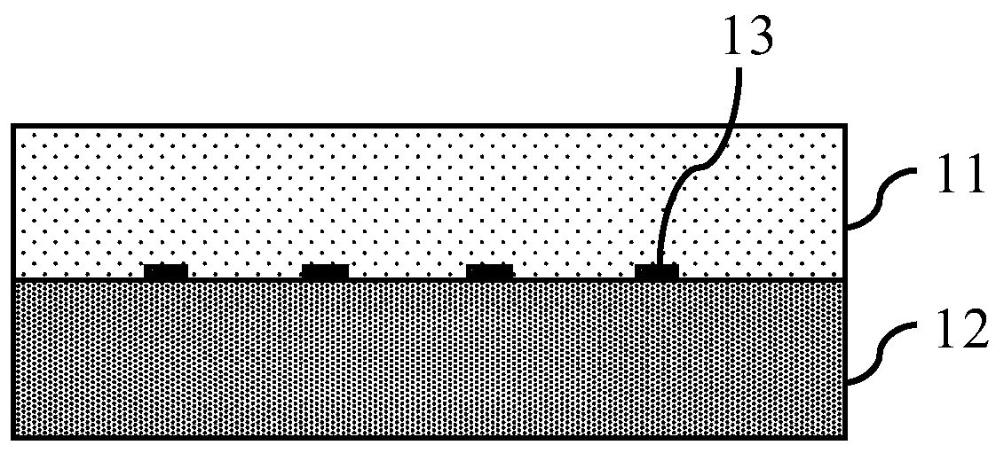
[0046] An embodiment of the present invention provides a method for manufacturing a test piece, see figure 2 , figure 2 It is a flow chart of a method for manufacturing a test piece according to an embodiment of the present invention. The test piece is used to detect deformation defects in a wafer bonding structure caused by a wafer bonding machine. The method for manufacturing the test piece...


PUM


Abstract

The invention provides a test piece, a manufacturing method thereof, a wafer bonding defect detection method detection method and a manufacturing method of a semiconductor device. The test piece and asecond wafer are placed on a wafer bonding machine table so as to be bonded to form a wafer bonded structure; a bonding pattern on the test piece is located on the top surface of the wafer bonded structure; and the bonding pattern on the top surface of the wafer bonded structure is scanned, and the distribution condition of deformation defects in the wafer bonded structure is obtained according to a scanning result and the front value coordinates of the bonding pattern on the test piece, so that whether the deformation parameters of the wafer bonding machine table are abnormal or not can be quickly and accurately detected; and therefore, batch product abnormities are avoided.

Description

technical field [0001] The invention relates to the technical field of semiconductor manufacturing, in particular to a test piece and its manufacturing method, a wafer bonding defect detection method and a semiconductor device manufacturing method. Background technique [0002] The distortion parameter is a very important parameter of the wafer bonding machine. Once the performance of the distortion parameter deviates (performance shift), it will lead to abnormalities in the subsequent process. Therefore, it is necessary to quickly and accurately detect the performance of the deformation parameters of the wafer bonding machine, find out the faulty parts on the machine in time and make improvements to avoid abnormal batch products. [0003] At present, the method of detecting whether the deformation parameters of the wafer bonding machine are abnormal is: prepare a fast processing batch, quickly carry out the subsequent process after the wafer bonding, until the thinning proc...

Claims


Application Information

Patent Timeline
IPC IPC(8): H01L23/544H01L21/66H01L21/67G01B11/16G01N21/95
CPCG01B11/16G01N21/9501H01L21/67288H01L22/12H01L22/30
Inventor 姚佳辉
Owner WUHAN XINXIN SEMICON MFG CO LTD
Features
  • R&D
  • Intellectual Property
  • Life Sciences
  • Materials
  • Tech Scout
  • Unparalleled Data Quality
  • Higher Quality Content
  • 60% Fewer Hallucinations
Learn More