Back-lighting-type near-infrared pixel unit and manufacturing method thereof

A pixel unit and near-infrared technology, applied in the field of image sensors, can solve problems such as the inability of lithography machines to penetrate effectively, the inability to realize the alignment of silicon wafer backside graphics and front-side transistors, and affect the performance of near-infrared pixel units, so as to improve epitaxy. Layer thickness, effect of increasing photosensitivity

Active Publication Date: 2019-12-31
CHENGDU LIGHT COLLECTOR TECH
View PDF4 Cites 0 Cited by
  • Summary
  • Abstract
  • Description
  • Claims
  • Application Information

AI Technical Summary

Problems solved by technology

However, the limit of the silicon layer that the lithography machine can penetrate is 5 microns, so when the epitaxial layer of tens to hundreds of microns is used, the lithography machine can no longer penetrate effectively, and it is impossible to achieve the alignment of the pattern on the back of the silicon wafer and the front transistor. Thus affecting the performance of the near-infrared pixel unit

Method used


Image

  • Back-lighting-type near-infrared pixel unit and manufacturing method thereof
  • Back-lighting-type near-infrared pixel unit and manufacturing method thereof
  • Back-lighting-type near-infrared pixel unit and manufacturing method thereof

Examples


Embodiment Construction

[0033] In order to make the purpose, technical solution and advantages of the present invention clearer, the specific implementation manners of the present invention will be further described in detail below in conjunction with the accompanying drawings.

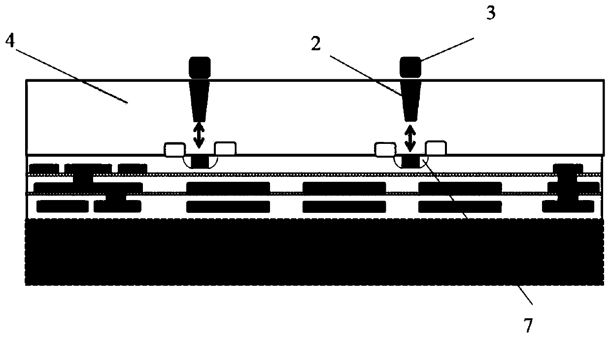
[0034] as attached figure 1 As shown, since the thickness of the epitaxial layer 4 required in the near-infrared pixel unit is tens or even hundreds of microns, and under this thickness, the photolithography machine cannot isolate the front transistor 7 at the bottom of the silicon layer from the back trench at the top of the silicon layer 2 and the back metal isolation 3 are aligned, thereby affecting the normal operation of the near-infrared pixel unit.

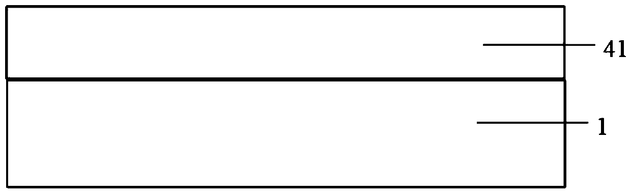
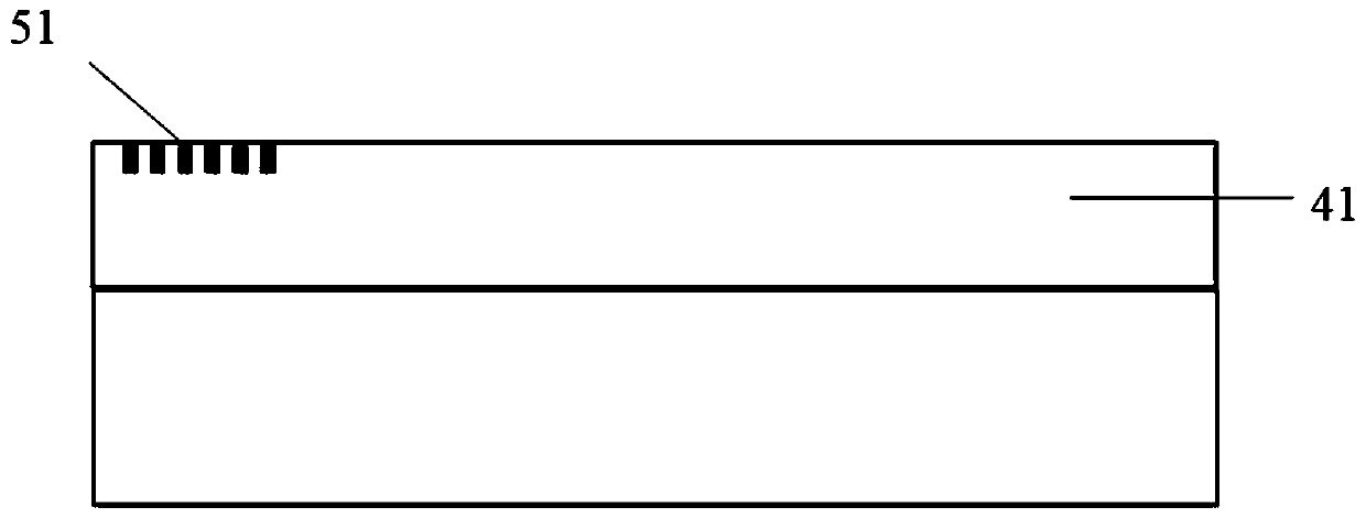
[0035] as attached Figure 9 As shown, a back-illuminated near-infrared pixel unit provided by the present invention includes a carrier 8, a front device 11, an epitaxial layer, and a rear device 12, wherein the epitaxial layer includes a first epitaxial layer 41, a seco...


PUM

PropertyMeasurementUnit
Thicknessaaaaaaaaaa

Abstract

The invention discloses a manufacturing method of a back-lighting-type near-infrared pixel unit. The method comprises the following steps of S01, preparing a substrate, epitaxially generating a firstepitaxial layer on a surface of the substrate, and forming a first alignment mark on the surface of the first epitaxial layer; S02, epitaxially generating a second epitaxial layer on the surface of the first epitaxial layer, and forming a second alignment mark aligned with the first alignment mark on the surface of the second epitaxial layer; S03, repeating the step S02 till that an Nth epitaxiallayer and an Nth alignment mark are generated; S04, forming a front device on the surface of the Nth epitaxial layer; S05, inverting the substrate, and bonding the front device with slide glass; and S06, removing the substrate, and exposing the first epitaxial layer; and forming a back device on the surface of the exposed first epitaxial layer, wherein the back device is aligned with the front device through the first epitaxial layer, the second epitaxial layer until the Nth epitaxial layer. By using the back-lighting-type near-infrared pixel unit and the manufacturing method thereof, a thickness of the epitaxial layer of the back-lighting-type near-infrared pixel unit can be increased.

Description

technical field [0001] The invention relates to the field of image sensors, in particular to a back-illuminated near-infrared pixel unit and a preparation method thereof. Background technique [0002] An image sensor refers to a device that converts optical signals into electrical signals. Generally, large-scale commercial image sensor chips include charge-coupled device (CCD) image sensors and complementary metal-oxide semiconductor (CMOS) image sensor chips. Compared with traditional CCD image sensors, CMOS image sensors have the characteristics of low power consumption, low cost, and compatibility with CMOS technology, so they are more and more widely used. Now CMOS image sensors are not only used in consumer electronics such as miniature digital cameras (DSC), mobile phone cameras, video cameras and digital single-lens reflex (DSLR), but also in automotive electronics, monitoring, biotechnology and medical fields. [0003] In current applications such as security monito...

Claims


Application Information

Patent Timeline
IPC IPC(8): H01L27/146H01L23/544
CPCH01L23/544H01L27/1464H01L27/14649H01L27/14683H01L2223/54426
Inventor 王勇
Owner CHENGDU LIGHT COLLECTOR TECH
Why Eureka
Try Eureka