Feeding and conveying device of semiconductor chip sorting and testing device, and working method thereof

A technology of conveying device and testing device, which is applied in the direction of measuring device, electronic circuit test, automatic test system, etc. It can solve problems such as chip damage, lower yield rate, and unsuitability for high-end chips with precision requirements, so as to reduce production consumption and improve yield efficiency, less friction

Pending Publication Date: 2020-01-03
扬州泽旭电子科技有限责任公司
View PDF1 Cites 5 Cited by
  • Summary
  • Abstract
  • Description
  • Claims
  • Application Information

AI Technical Summary

Problems solved by technology

As mentioned above, integrated circuit chips are scattered in the vibrating tray. During the vibration process, the mutual friction between the chips will cause damage to the chips and reduce the yield rate. Therefore, this solution is only suitable for chips with low precision requirements. , not suitable for high-end chips with high precision requirements

Method used


Image

  • Feeding and conveying device of semiconductor chip sorting and testing device, and working method thereof
  • Feeding and conveying device of semiconductor chip sorting and testing device, and working method thereof
  • Feeding and conveying device of semiconductor chip sorting and testing device, and working method thereof

Examples


Embodiment Construction

[0053] Below, the present invention will be further described in conjunction with the accompanying drawings and specific implementation methods. It should be noted that, under the premise of not conflicting, the various embodiments described below or the technical features can be combined arbitrarily to form new embodiments. .

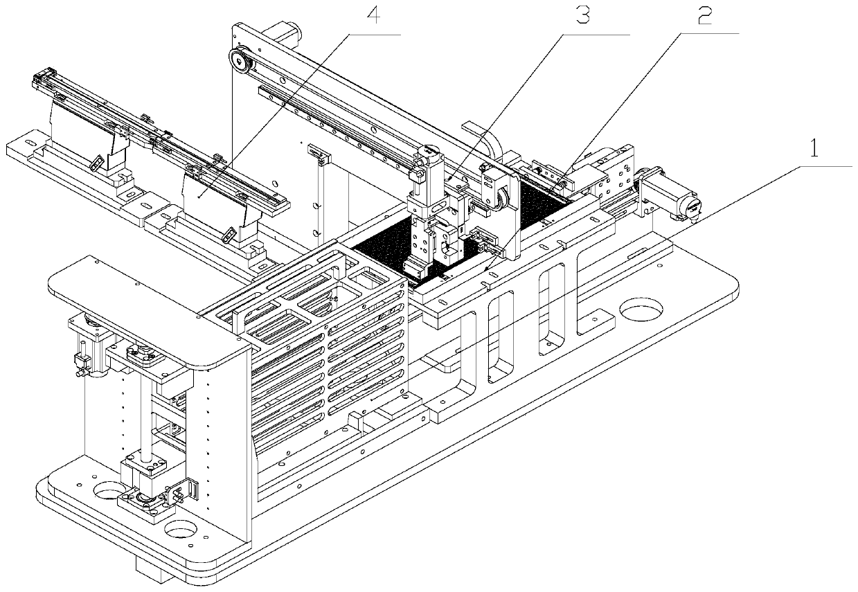
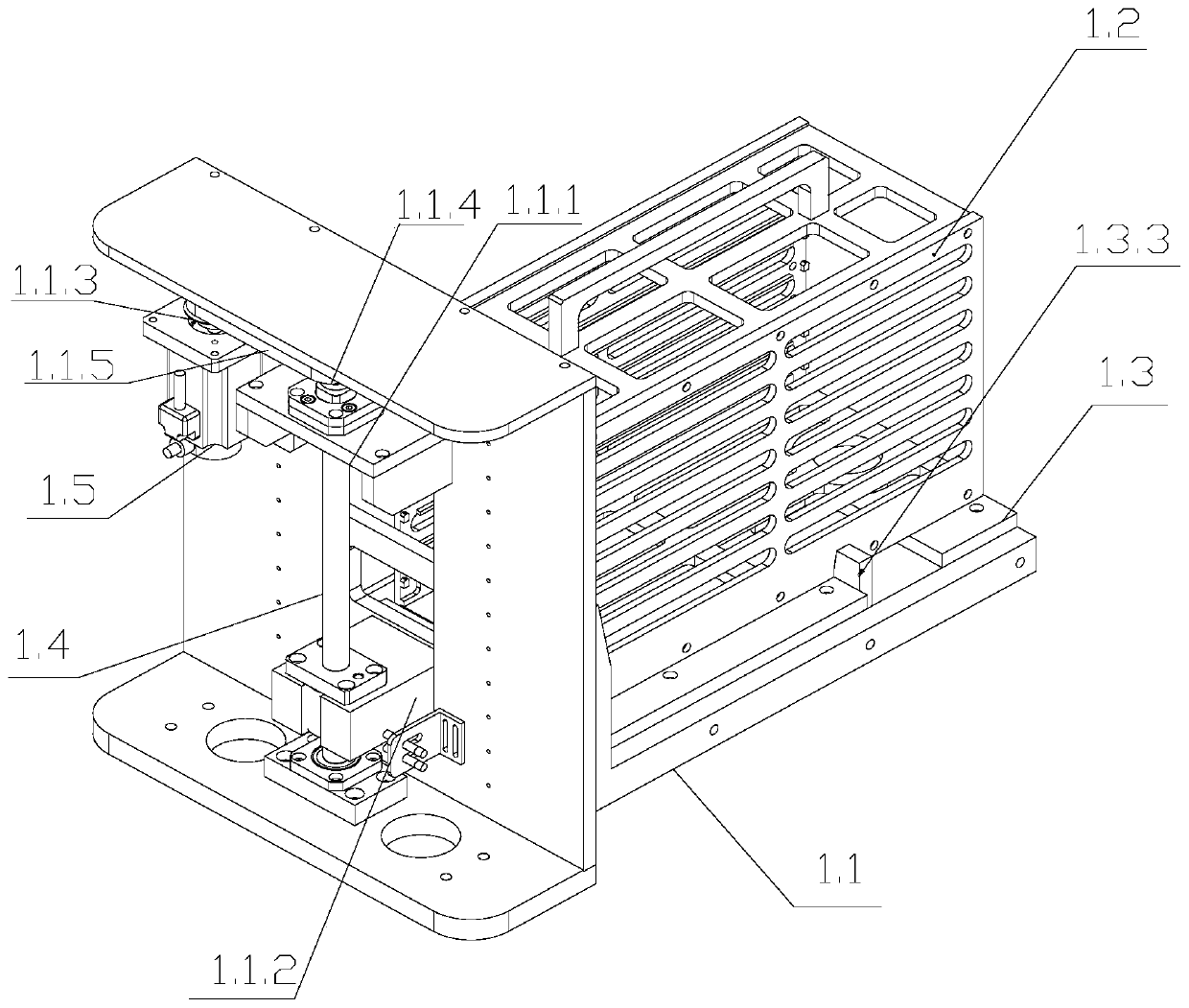
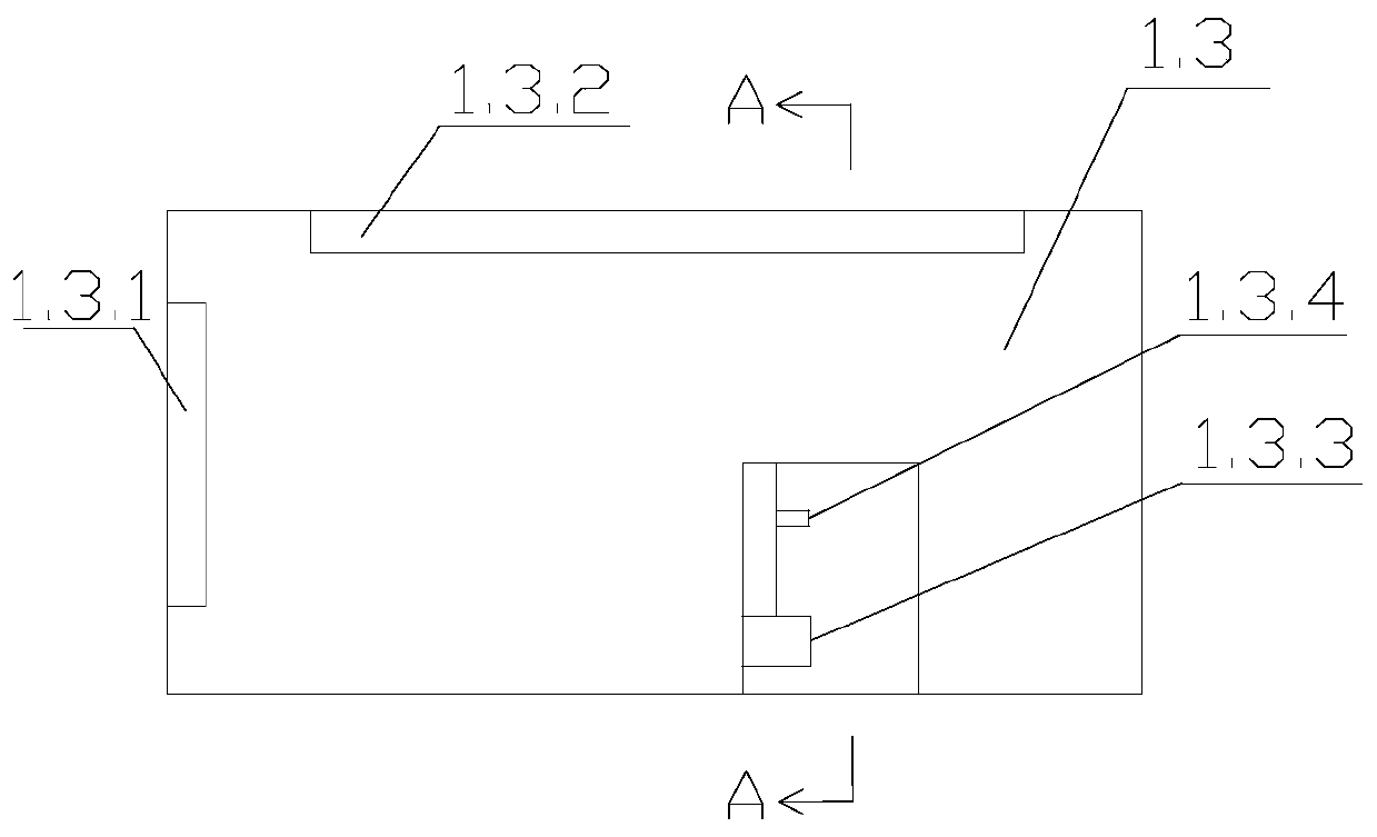
[0054] Such as Figure 1-11 Shown, a kind of feeding and conveying device of semiconductor chip sorting and testing device, comprises the tray loading and feeding device 1 that is positioned on the workbench, takes tray device 2, takes chip device 3 and chip conveying device 4, as figure 2 As shown, the feeding device includes an L-shaped support 1.1, a basket 1.2 positioned on the support 1.1 and a lifting device for the basket 1.2, and the lifting device includes a horizontally arranged basket supporting plate 1.3, a vertical The ball screw 1.4 and the servo motor 1.5 are arranged vertically, the basket support plate 1.3 is located on the horizonta...


PUM


Abstract

The invention provides a feeding and conveying device of a semiconductor chip sorting and testing device, which generates no damage to the chip and has a high automation degree, and a working method thereof. The feeding and conveying device comprises a tray feeding device located on a worktable, a tray taking device, a chip taking device and a chip conveying device, the tray feeding device is responsible for raising a tray to a suitable position to enable the tray taking device to take out the tray, the tray taking device is responsible for taking out trays in a lifting basket one by one for enabling the chip taking device to take out chips, the chip taking device is responsible for taking out the chips in the trays and conveying the chips into the chip conveying device, and the chip conveying device is responsible for conveying the chips to a detection station. The chips in the feeding and conveying device provided by the invention are subjected to less collision and friction, the yield of the chips is greatly improved, and the production consumption is reduced, so that the production cost is reduced.

Description

technical field [0001] The invention relates to the technical field of semiconductor chip sorting and testing equipment, in particular to a material feeding and conveying device of a semiconductor chip sorting and testing device and a working method thereof. Background technique [0002] Integrated circuit turntable high-speed test and sorting equipment is a high-end key equipment in the post-process of modern electronic manufacturing industry. It has the advantages of fast speed, high sorting efficiency, and powerful function integration. Among them, the feeding device is used to complete chip-related function testing. The key components. [0003] The invention patent titled "a device for testing and sorting integrated circuit chips" and application number "201821652888.7" discloses a device for testing and sorting integrated circuit chips. There is a turret system, and there are several functional stations around the turret system. Automatic feeding system, positioning sy...

Claims


Application Information

Patent Timeline
Patent Type & Authority Applications(China)
IPC IPC(8): G01R31/28G01R31/01B07C5/02
CPCB07C5/02G01R31/01G01R31/2834G01R31/2893
Inventor 李永备潘小华芦俊
Owner 扬州泽旭电子科技有限责任公司
Why Eureka
Try Eureka