Fast recovery diode

A recovery diode and silicon dioxide technology, which is applied in the direction of electrical components, circuits, semiconductor devices, etc., can solve the problems of inability to produce fast recovery diode chips, difficulty in achieving extremely low Trr, and difficulty in leakage current control, etc., to achieve fast turn-on and Effect of turn-off capability, low current oscillation and voltage overshoot, short reverse recovery time

Pending Publication Date: 2020-01-14
YANGZHOU GUOYU ELECTRONICS
View PDF1 Cites 1 Cited by
  • Summary
  • Abstract
  • Description
  • Claims
  • Application Information

AI Technical Summary

Problems solved by technology

At present, domestic chip manufacturers can use P- / N- / N+ structure to manufacture fast recovery diode chips with faster reverse recovery time, and can also use P- / N- / N / N+ structure to manufacture low-oscillation fast recovery diodes For the chip, the reverse recovery time of the former is extremely short, but the shock is severe, while the latter has almost no shock, but it is difficult to achieve an extremely low Trr
Restricted by high-end production equipment, domestic chip manufacturers cannot produce fast recovery diode chips with high frequency and low oscillation performance, so such fast recovery diode chips mainly rely on imports
[0003] An invention patent is disclosed in the prior art, patent name: a fast recovery diode chip with low reverse recovery charge, patent number: CN201510951716.4, but in the above patent disclosure, in order to achieve a very fast recovery speed, it is necessary to improve The concentration of the diode doped with platinum or gold, as the doping concentration increases, it becomes very difficult to control the leakage current when using the mesa glass passivation process

Method used


Image

  • Fast recovery diode
  • Fast recovery diode

Examples


Embodiment

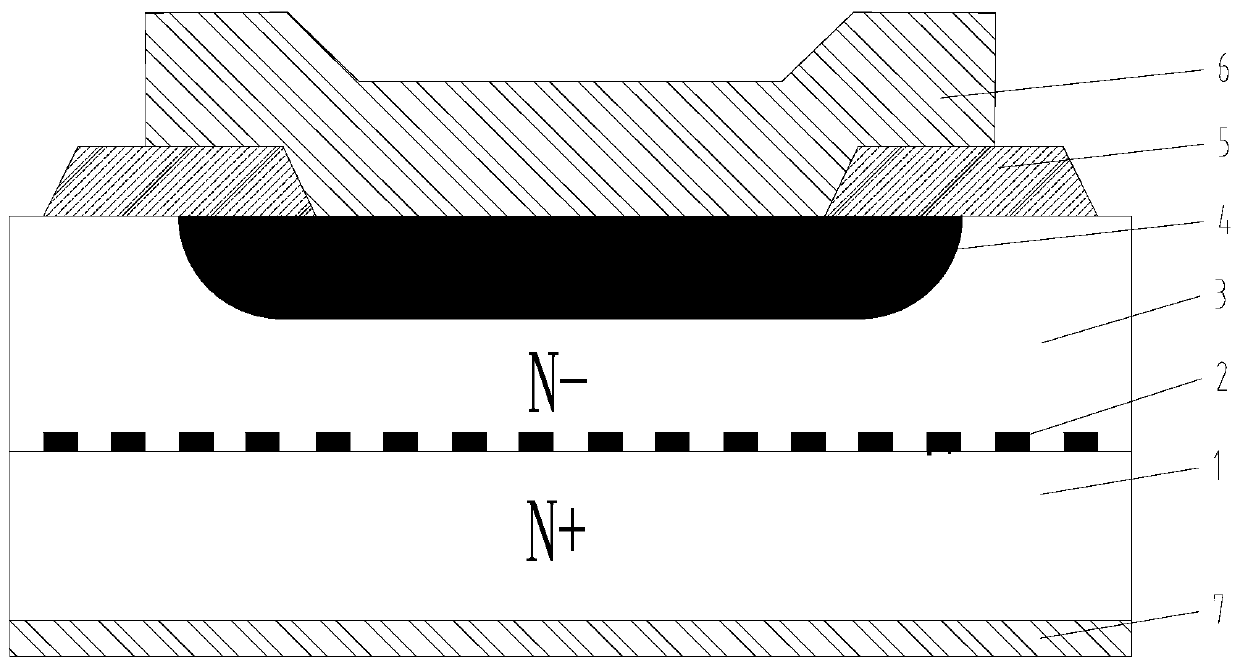
[0022] Example: such as figure 1 As shown, a fast recovery diode includes an N+ type silicon single crystal substrate 1, a P+ type cylinder 2, an N-type epitaxial layer 3, a P-type main junction 4, a silicon dioxide layer 5, a front metal layer 6 and a back surface A metal layer 7, a back metal layer 7 is arranged under the N+ type silicon single crystal substrate 1, a plurality of P+ type cylinders 2 are arranged above the N+ type silicon single crystal substrate 1, and an N- type epitaxial layer is arranged above the P+ type cylinder 2 3. A P-type main junction 4 is arranged above the N-type epitaxial layer 3, the P-type main junction 4 is arranged in the N-type epitaxial layer 3, and a front metal layer 6 is arranged above the P-type main junction 4. N- A silicon dioxide layer 5 is provided between the type epitaxial layer 3 and the front metal layer 6, and the silicon dioxide layer 5 is provided with a through hole matching the P-type main junction 4.

[0023] Among them: N+ ...


PUM

PropertyMeasurementUnit
depthaaaaaaaaaa
depthaaaaaaaaaa
electrical resistivityaaaaaaaaaa

Abstract

The invention discloses a fast recovery diode in the field of semiconductor power devices. The fast recovery diode includes an N+ type of silicon single crystal substrate, an N- type of epitaxial layer, a plurality of P+ type of blocks, and a P- type of main junction. The N- type of epitaxial layer is disposed above the N+ type of silicon single crystal substrate. The P- type of main junction is disposed above the N- type of epitaxial layer. The P+ type of blocks are arranged between the N+ type of silicon single crystal substrate and the N- type of epitaxial layer. A front metal layer is disposed above the P- type of main junction. A back metal layer is disposed under the N+ type of silicon single crystal substrate. The fast recovery diode has extremely short reverse recovery time, fast turn-on and turn-off capabilities, has extremely low current oscillation and voltage overshoot, and improves the stability and reliability of a device.

Description

Technical field [0001] The present invention relates to the technical field of semiconductor power devices, in particular to a fast recovery diode. Background technique [0002] As the core device in power electronic circuits, power semiconductor devices can be used to realize efficient transmission and conversion of electric energy and effective and precise control in the process, and realize high-quality and efficient utilization of electric energy. It is precisely because of the research and development of power semiconductor devices that power electronics technology develops in the direction of large capacity, high frequency, high efficiency, energy saving, high reliability and low cost. Due to the development of high-frequency conversion technology and the need for high-efficiency and energy-saving, fast recovery diodes are required to have strong high-voltage blocking capabilities and fast switching speeds. With the increasing renewal of circuit structures, circuit designe...

Claims


Application Information

Patent Timeline
Patent Type & Authority Applications(China)
IPC IPC(8): H01L29/868H01L29/06
CPCH01L29/0615H01L29/868
Inventor 王源政金银萍杭圣桥郁怀东
Owner YANGZHOU GUOYU ELECTRONICS
Why Eureka
Try Eureka