
LDMOS device and manufacturing method thereof

A manufacturing method and device technology, which is applied in the field of laterally diffused metal oxide semiconductor devices, can solve the problems of reduced efficiency and power consumption of LDMOS devices, and achieve the effects of small gap, low ohmic loss, and improved breakdown voltage

Inactive Publication Date: 2020-01-21
CHENGDU MONOLITHIC POWER SYST
View PDF10 Cites 0 Cited by
  • Summary
  • Abstract
  • Description
  • Claims
  • Application Information

AI Technical Summary

Problems solved by technology

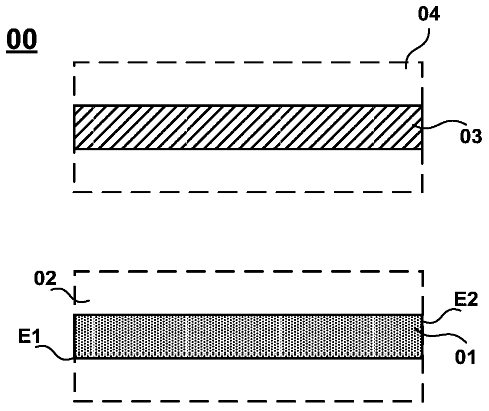
[0003] A disadvantage of the above structure is that since the field plate contact metal layer 02 and the drain contact metal layer 04 are parallel, fringing fields will be generated, and the fringing fields make the field plate contact metal layer 02 and the drain contact metal layer 04 A parasitic capacitance is generated between the LDMOS device, which causes the power consumption of the LDMOS device during switching, and its efficiency is reduced

Method used


Image

  • LDMOS device and manufacturing method thereof
  • LDMOS device and manufacturing method thereof
  • LDMOS device and manufacturing method thereof

Examples


Embodiment Construction

[0014] Specific embodiments of the present invention will be described in detail below, and it should be noted that the embodiments described here are only used for illustration and are not intended to limit the present invention. In the following description, numerous specific details are set forth in order to provide a thorough understanding of the present invention. It will be apparent, however, to one of ordinary skill in the art that these specific details need not be employed to practice the present invention. In other instances, well-known circuits, materials or methods have not been described in detail in order to avoid obscuring the present invention.

[0015] Throughout this specification, reference to "one embodiment," "an embodiment," "an example," or "example" means that a particular feature, structure, or characteristic described in connection with the embodiment or example is included in the present invention. In at least one embodiment. Thus, appearances of t...


PUM


Abstract

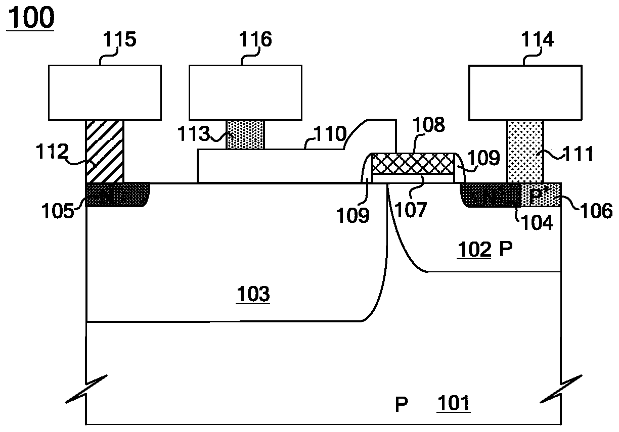
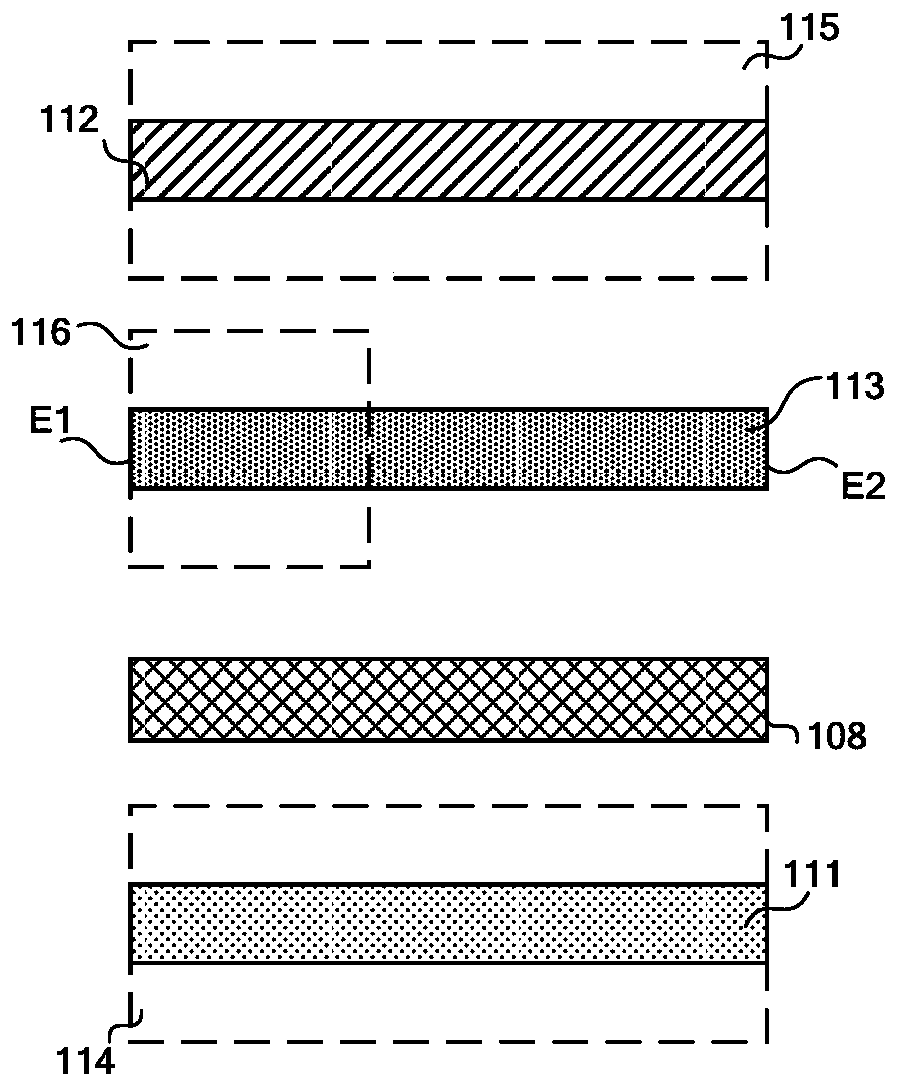
The invention discloses an LDMOS device and a manufacturing method thereof. The LDMOS device includes a source region and a drain region in a substrate and a gate on the substrate laterally between the source region and the drain region. The LDMOS device also includes a field plate in a region between the gate and the drain region on the substrate and a field plate contact on the field plate. Thefield plate contact includes an upper surface including a first portion and a second portion in a longitudinal direction. The upper surface of the field plate contact also electrically contacts a field plate contact metal layer that covers the first portion of the field plate contact and does not cover the second portion of the field plate contact. Thus, the area of the field plate contact metal layer is reduced, the fringe field between the field plate contact metal layer and the drain metal layer is reduced, and the parasitic capacitance between the two is reduced. Therefore, the peak electric field is effectively reduced, or the breakdown voltage of the LDMOS device is effectively improved.

Description

technical field [0001] The present invention relates to a laterally diffused metal oxide semiconductor (Laterally Diffused Metal Oxide Semiconductor, LDMOS) device, in particular to a field plate contact (field plate contact) and a field plate contact metal layer (field plate contact metal layer) of the LDMOS device. Background technique [0002] At present, field plates of various structures are widely used in semiconductor devices to effectively reduce the peak electric field at a given voltage, or to effectively increase the breakdown voltage when the critical electric field is reached. FIG. 1 shows a top view of a partial structure of a conventional LDMOS device 00. Such as figure 1 As shown, the LDMOS device 00 includes a field plate contact 01 over a field plate (not shown) and a field plate contact metal layer 02 over the field plate contact 01 . Wherein, the field plate contact 01 is parallel to the drain contact 03 in the longitudinal direction. A drain contact m...

Claims


Application Information

Patent Timeline
Patent Type & Authority Applications(China)
IPC IPC(8): H01L29/40H01L29/417H01L29/78H01L21/336H01L21/28
CPCH01L29/7816H01L29/402H01L29/41725H01L29/66681H01L29/401H01L29/7835H01L29/66659H01L29/1045H01L29/0692H01L21/823871H01L29/0878H01L29/0865H01L29/0882H01L29/086
Inventor 艾瑞克·布劳恩乔伊·迈克格雷格郑志星
Owner CHENGDU MONOLITHIC POWER SYST
Learn More