
Flattening process method

A planarization process and process technology, applied in the field of planarization process, can solve problems such as reducing the performance of semiconductor devices, and achieve the effect of ensuring height and size

Active Publication Date: 2022-07-12
SEMICON MFG INT (SHANGHAI) CORP +1
View PDF6 Cites 0 Cited by
  • Summary
  • Abstract
  • Description
  • Claims
  • Application Information

AI Technical Summary

Problems solved by technology

[0003] However, in the actual process, the height of the final metal gate structure is easily lower than the set target height, which reduces the performance of semiconductor devices

Method used


Image

  • Flattening process method
  • Flattening process method
  • Flattening process method

Examples


no. 1 example

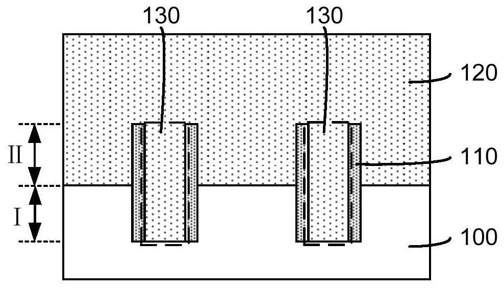
[0035] Please refer to figure 1 , a metal material layer 120 is formed on the semiconductor substrate 100 , and a metal gate 130 is formed in the semiconductor substrate 100 and the metal material layer 120 .

[0036] The semiconductor substrate 100 serves as a process basis for forming semiconductor devices. The material of the semiconductor substrate 100 is at least one of the following materials: polysilicon, silicon-on-insulator (SOI), silicon-on-insulator (SSOI), silicon-germanium-on-insulator (S-SiGeOI), and silicon-on-insulator (S-SiGeOI) Silicon germanium (SiGeOI), etc. In the embodiment of the present invention, the material of the semiconductor substrate 100 is polysilicon, and the semiconductor substrate 100 also includes other structures, such as: metal plugs, metal connection layers, dielectric layers and other structures, or includes these structures. other semiconductor devices, which are not specifically limited here.

[0037] In the embodiment of the prese...

no. 2 example

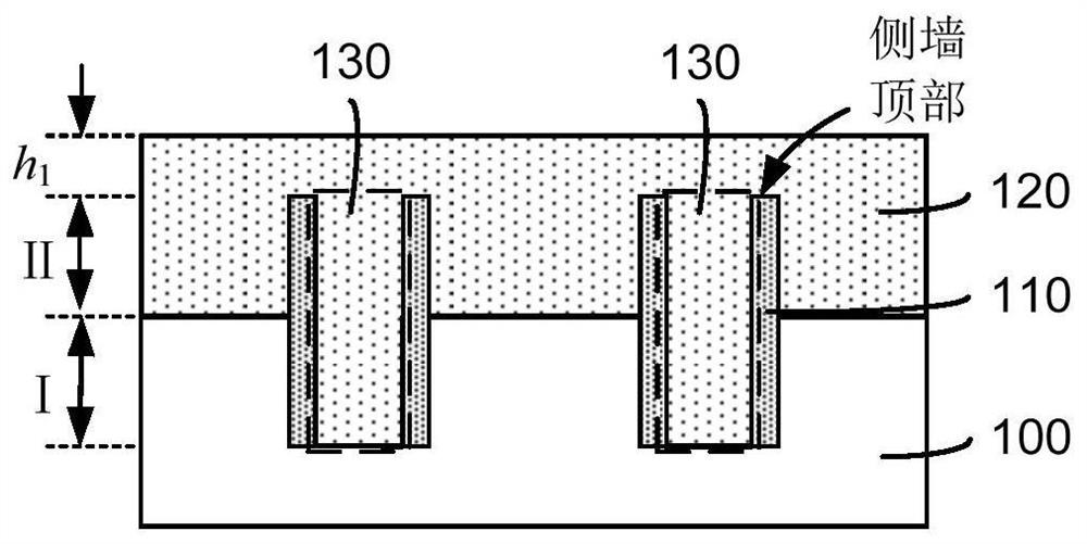
[0072] The difference between the second embodiment and the first embodiment is that the first grinding process is used to directly grind the metal material layer, the sidewall spacers and the second part of part of the metal gate, so that the second part of the remaining metal gate has the first a height. The subsequent process steps are the same as in the first embodiment.

[0073] Please refer to Image 6 , providing a semiconductor substrate 200 , a spacer 210 , a metal material layer 220 and a metal gate 230 .

[0074] The structures, functions and positional relationships of the semiconductor substrate 200 , the sidewall spacers 210 , the metal material layer 220 and the metal gate 230 are the same as those of the first embodiment, and are not repeated here.

[0075] Please refer to Figure 7 , using the first grinding process to grind the metal material layer 220 , part of the second part of the metal gate 230 and the sidewall spacer 210 .

[0076] The purpose of pe...


PUM


Abstract

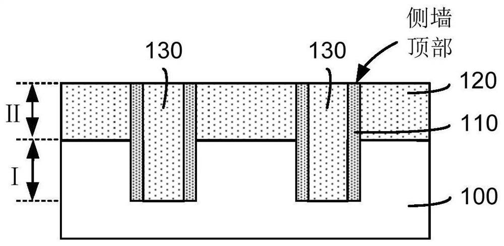
A planarization process method includes: providing a semiconductor substrate and a metal material layer, the metal material layer is arranged above the semiconductor substrate, a metal gate and a sidewall are formed in the semiconductor substrate and the metal material layer, and the sidewall is formed on the metal The two side walls of the gate, the first part of the metal gate is formed in the semiconductor substrate, and the second part of the metal gate is formed in the metal material layer; the first grinding process is used to grind the metal material layer, or grind part of the sidewall, the second part of the metal gate, so that the second part of the remaining metal gate has a first height; and performing a second grinding process on the remaining metal gate and the sidewall spacers, exposing the semiconductor substrate, the first grinding process and the second grinding process The grinding process has a grinding rate ratio for the metal material layer or metal gate and for the sidewall spacer, respectively. Grinding the second portion of the metal gate in a two-step process allows for fine control over the height dimension of the final metal gate structure.

Description

technical field [0001] The present invention relates to the field of semiconductor manufacturing, in particular to a planarization process method. Background technique [0002] In the semiconductor device manufacturing process, after the groove is filled with metal material, it is necessary to perform grinding to remove excess metal material, and to planarize the surface of the metal material layer to facilitate subsequent deposition of other materials. For example, in the process of forming the metal gate, the top of the metal material is generally higher than the top of the metal gate, and a chemical mechanical planarization process method is used to control the height of the metal gate. [0003] However, in an actual process, the height of the final metal gate structure is likely to be lower than the set target height, which reduces the performance of the semiconductor device. [0004] Therefore, there is an urgent need for a planarization process method for controlling ...

Claims


Application Information

Patent Timeline
Patent Type & Authority Patents(China)
IPC IPC(8): H01L21/306H01L21/321
CPCH01L21/30625H01L21/3212
Inventor 纪登峰金懿张庆刘璐蒋莉
Owner SEMICON MFG INT (SHANGHAI) CORP
Learn More