Supercharge Your Innovation With Domain-Expert AI Agents!

Side wall electrode resistive random access memory structure and preparation method thereof

A resistive variable storage and electrode technology, which is applied in the field of memory, can solve the problems of difficult control of etching morphology, limited height of through holes, and difficult etching process, etc., and achieve the advantages of embedded integration, size reduction, and height reduction Effect

Active Publication Date: 2020-02-04
HANGZHOU WEIMING XINKE TECH CO LTD +1
View PDF14 Cites 1 Cited by
  • Summary
  • Abstract
  • Description
  • Claims
  • Application Information

AI Technical Summary

Problems solved by technology

Traditional sandwich RRAM devices such as figure 1 As shown, in order to ensure the electrical performance of RRAM devices, there are certain requirements for the thickness of the bottom electrode-resistive layer-top electrode. The height of via holes in the back stage of advanced process nodes is limited, which poses a great challenge to the uniformity of each layer of RRAM and device performance
Moreover, the etching process of multilayer metal is difficult, and the etching morphology is difficult to control in an ideal situation, and the O in etching 2 The gas will further oxidize the resistive variable layer, and these unfavorable factors limit the manufacture of RRAM devices

Method used


Image

  • Side wall electrode resistive random access memory structure and preparation method thereof
  • Side wall electrode resistive random access memory structure and preparation method thereof
  • Side wall electrode resistive random access memory structure and preparation method thereof

Examples


preparation example Construction

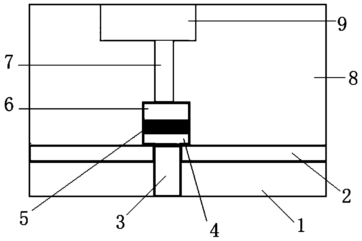
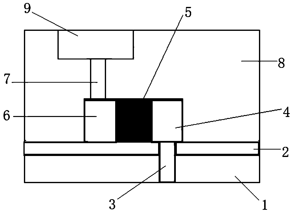
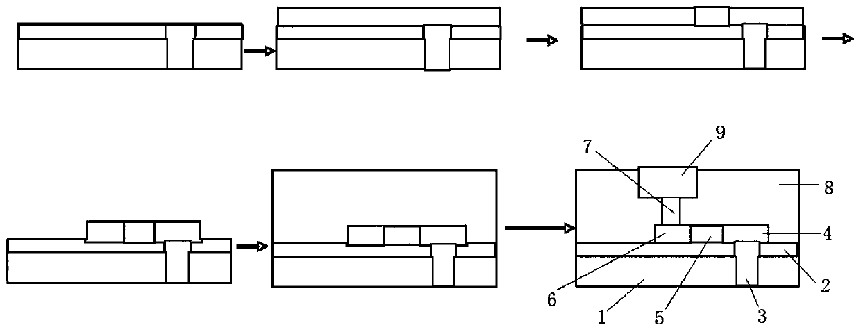
[0047] This embodiment also provides a method for preparing a sidewall electrode resistive memory structure, including:

[0048] S1. Providing a first dielectric layer;

[0049] S2. Depositing and forming a low-mobility material layer on the first dielectric layer;

[0050]S3. Prepare a first through hole penetrating through the low mobility material layer and the first dielectric layer;

[0051] S4. Forming a first metal plug in the first through hole;

[0052] S5. Depositing an electrode material layer on the low mobility material layer;

[0053] S6. Open a channel on the electrode material layer that penetrates up and down and divides the electrode material layer into left and right parts, and deposits a resistive material in the channel to form a resistive layer;

[0054] S7, patterning the electrode material layer to form a first electrode and a second electrode.

[0055] In some embodiments, the method also includes:

[0056] S8. Depositing and forming a second diel...


PUM

PropertyMeasurementUnit
thicknessaaaaaaaaaa

Abstract

The invention discloses a side wall electrode resistive random access memory structure and a preparation method thereof. The structure comprises a first dielectric layer, a low-mobility material layer, a first metal plug, a first electrode, a resistive random access layer and a second electrode, wherein the low-mobility material layer is arranged on the first dielectric layer; the first electrodeand the resistive random access layer are arranged on the low-mobility material layer; the first electrode, the resistive random access layer and the second electrode are sequentially connected; the first metal plug penetrates through the first dielectric layer and the low-mobility material layer, and the upper end of the first metal plug is connected with the first electrode. According to the side wall electrode resistive random access memory structure provided by the embodiment of the invention, at least one electrode is arranged on one side of the resistive random access layer in the horizontal direction. Compared with the prior art, the height of the resistive random access memory structure is reduced, the size of the RRAM is reduced, and embedded integration of the RRAM is facilitated.

Description

technical field [0001] The invention relates to the field of memory technology, in particular to a sidewall electrode resistive memory structure and a preparation method thereof. Background technique [0002] Resistive Random Access Memory (RRAM), also called Resistive Random Access Memory (RRAM), is a non-volatile memory device that records and stores data information based on resistance changes. Because of its high density, low cost, fast access speed and breakthrough technology development, resistive memory is considered to be a strong competitor for the next generation of new memory. It has great potential in embedded devices, AI fields, edge computing fields, etc. Very broad application prospects. Traditional sandwich RRAM devices such as figure 1 As shown, in order to ensure the electrical performance of RRAM devices, there are certain requirements for the thickness of the bottom electrode-resistive layer-top electrode. The height of through holes in the back stage ...

Claims


Application Information

Patent Timeline
Patent Type & Authority Applications(China)
IPC IPC(8): H01L45/00
CPCH10N70/841H10N70/011
Inventor 肖韩王宗巍蔡一茂
Owner HANGZHOU WEIMING XINKE TECH CO LTD
Features
  • R&D
  • Intellectual Property
  • Life Sciences
  • Materials
  • Tech Scout
  • Unparalleled Data Quality
  • Higher Quality Content
  • 60% Fewer Hallucinations
Learn More