An array integrated micro LED chip and its manufacturing method

A LED chip and miniature technology, which is applied in the direction of semiconductor devices, electrical components, circuits, etc., can solve the problems of high transfer accuracy requirements, low transfer process yield, and low transfer yield, so as to improve integration and utilization, Improve packaging efficiency and yield, and solve the effect of low efficiency

Active Publication Date: 2020-09-01
FOSHAN NATIONSTAR SEMICON
View PDF7 Cites 0 Cited by
  • Summary
  • Abstract
  • Description
  • Claims
  • Application Information

AI Technical Summary

Problems solved by technology

As the application of LED displays in the display field becomes more and more popular, the red, green and blue LED chips and the spacing between the chips also need to be continuously reduced. When the LED chip is reduced to less than 100 μm, the chip The size has far exceeded the technological limit of the traditional chip transfer method. Therefore, at present, the mass transfer method of many tiny chips is used in the industry for batch transfer. However, this transfer method still has low transfer yield and extremely high transfer accuracy requirements. High, low yield in the transfer process, etc.

Method used


Image

  • An array integrated micro LED chip and its manufacturing method
  • An array integrated micro LED chip and its manufacturing method
  • An array integrated micro LED chip and its manufacturing method

Examples


Embodiment 1

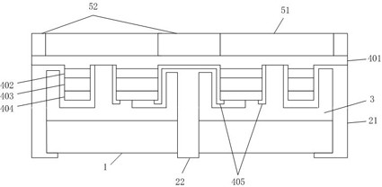
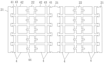
[0044] see figure 1 with figure 2, an array integrated micro LED chip provided by the present invention, comprising a substrate 1, a conductive connection layer, a thermosetting buffer layer 3 and n light emitting structures 4, the n light emitting structures 4 are divided into x rows and y columns, n>3, x>1, y>1; each light emitting structure 4 includes a first light emitting microstructure 41, a second light emitting microstructure 42 and a first isolation groove 43, and the first isolation groove 43 is arranged between the first light emitting microstructure 41 and the first light emitting microstructure 42. Between the second light-emitting microstructures 42; in the same row, a second isolation groove 44 is provided between two adjacent light-emitting structures 4; the conductive connection layer includes a first metal connection layer 21 and a second metal connection layer 22 , the first metal connection layer 21 forms a conductive connection to the first light-emittin...

Embodiment 2

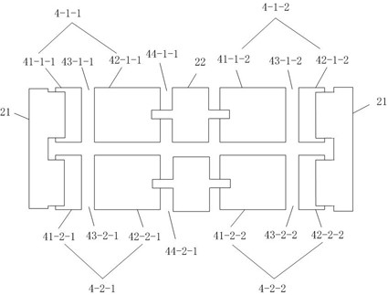
[0070] see image 3 , the LED chip of this embodiment includes 4 light-emitting structures, and the 4 light-emitting structures are divided into 2 rows and 2 columns, wherein the 2 light-emitting structures in the first row are marked as 4-1-1, 4-1-2 in sequence, and the second The two light emitting structures in the row are marked as 4-2-1 and 4-2-2 in turn, and the second isolation groove between the light emitting structures 4-1-1 and 4-1-2 in the first row is marked as 44-1 -1, the second isolation groove located between the light emitting structures 4-2-1 and 4-2-2 in the second row is marked as 44-2-1, and the second isolation grooves in the same column are connected.

[0071] Each light emitting structure includes a first light emitting microstructure, a second light emitting microstructure and a first isolation groove, wherein the light emitting structure 4-1-1 includes a first light emitting microstructure 41-1-1, a second light emitting microstructure 42 -1-1 and t...


PUM

PropertyMeasurementUnit
sizeaaaaaaaaaa

Abstract

The invention discloses an array integrated micro-LED chip and a manufacturing method thereof. The chip includes a substrate, a conductive connection layer, a thermosetting buffer layer and n light-emitting structures, and the conductive connection layer includes a first metal connection layer and a second metal connection layer. A connection layer, the first metal connection layer forms a conductive connection to the first light-emitting microstructures in the same row, and the second metal connection layer forms a conductive connection to two adjacent second light-emitting microstructures in the same row. The invention forms an integrated array of micro LED chips by means of all common cathodes and double common anodes, thereby improving the transfer efficiency and transfer yield of the chips.

Description

technical field [0001] The invention relates to the technical field of light-emitting diodes, in particular to an array-integrated micro-LED chip and a manufacturing method thereof. Background technique [0002] LED has a series of advantages such as energy saving, environmental protection, earthquake resistance and safety, and is widely used in lighting, display and other fields. As a high-tech product, LED display has attracted people's attention. Using computer control, the intelligent full-color display that integrates light and electricity has been widely used in advertising media, entertainment culture, traffic guidance, sports and other fields. For the application of LED display, the pixels are red, green and blue LED light-emitting diodes, which are arranged in a dot matrix, so as to realize the full-color display screen. As the application of LED display screens in the display field becomes more and more popular, the red, green and blue LED chips and the spacing be...

Claims


Application Information

Patent Timeline
Patent Type & Authority Patents(China)
IPC IPC(8): H01L25/075H01L33/00H01L33/48H01L33/54H01L33/60H01L33/62
CPCH01L25/0753H01L33/005H01L33/48H01L33/54H01L33/60H01L33/62
Inventor 徐亮雷自合
Owner FOSHAN NATIONSTAR SEMICON
Why Eureka
Try Eureka