Method for recovering threshold voltage reduction of MOSFET after irradiation

A technology of threshold voltage and irradiation, which is applied in the field of MOSFET, can solve the problems of low temperature threshold voltage, increase of turn-off loss, false turn-on of MOSFET, etc.

Pending Publication Date: 2020-02-11
SHENZHEN SANRISE TECH CO LTD
View PDF5 Cites 0 Cited by
  • Summary
  • Abstract
  • Description
  • Claims
  • Application Information

AI Technical Summary

Problems solved by technology

However, the threshold voltage drops too fast at high temperature, resulting in an increase in turn-off loss at high temperature.
The second is that during the switching process of the MOSFET, its gate will pass through C gd Coupling a certain voltage, if the threshold voltage of the MOSFET is too low, it will cause the MOSFET to turn on by mistake
These positive charges will also bring about the problem of lowering the high temperature threshold voltage

Method used


Image

  • Method for recovering threshold voltage reduction of MOSFET after irradiation
  • Method for recovering threshold voltage reduction of MOSFET after irradiation
  • Method for recovering threshold voltage reduction of MOSFET after irradiation

Examples


Embodiment Construction

[0028] The present invention will be described in detail below in conjunction with the accompanying drawings and specific embodiments.

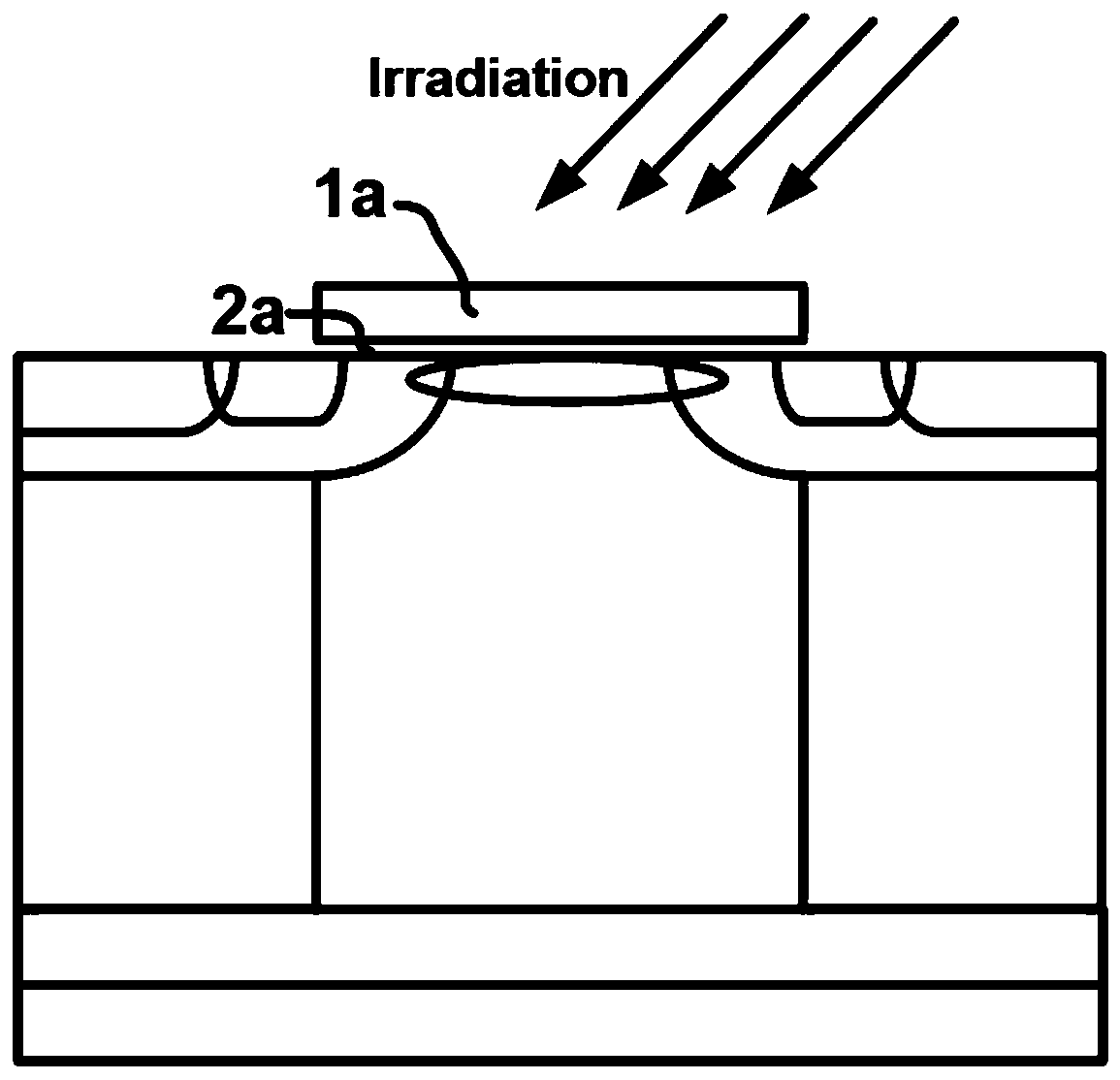
[0029] see Figure 4 , the present invention provides a method for recovering the lowering of MOSFET threshold voltage after irradiation, the method comprising the following steps: Step 1: providing a MOSFET, the MOSFET has undergone irradiation treatment; A voltage of a certain value is applied to the drain for a period of time, so that some electrons enter the oxide layer of the gate of the MOSFET and recombine with the trapped holes.

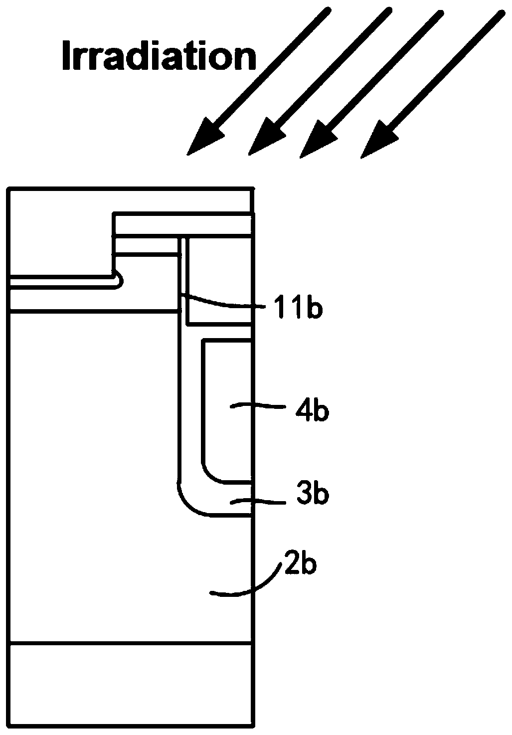
[0030] see Figure 5 , Figure 5 is a schematic diagram of an embodiment of applying a voltage to the gate of the MOSFET, in this embodiment, Figure 5 Among them, 1c is the gate of the MOSFET, and 2c is the oxide layer of the gate of the MOSFET. For the MOSFET of the silicon device, the oxide layer 2c of the gate is SiO 2 , the condition of the voltage applied to the gate 1c of the MOSFET can be: V gs ...


PUM

PropertyMeasurementUnit
thicknessaaaaaaaaaa
strengthaaaaaaaaaa

Abstract

The invention discloses a method for recovering the threshold voltage reduction of a MOSFET after irradiation. The method comprises the following steps: step 1, providing the MOSFET, wherein the MOSFET is irradiated; and step 2: applying a voltage of a certain value to the gate or the drain of the MOSFET for a period of time so that a part of electrons enter the oxide layer of the gate of the MOSFET and are recombined with the trapped holes. The voltage is applied to the gate or the drain of the irradiated MOSFET so that the electrons enter the oxide layer of the gate and are recombined with trapped holes, the threshold voltage of the device can be recovered and the problem of severe threshold voltage reduction of the MOSFET at high temperature can be alleviated.

Description

technical field [0001] The invention relates to the field of MOSFET technology, in particular to a method for recovering the lowered MOSFET threshold voltage after irradiation. Background technique [0002] MOSFET is a single-stage device, which is widely used in power conversion circuits due to its fast switching speed. How to improve the efficiency of MOSFET devices has always been the focus of industry research. In the design of MOSFET devices, the method of reducing the capacitance of MOSFET devices is mainly used, that is, in the case of the same on-resistance, the gate capacitance and gate-drain of MOSFET devices are reduced. Coupling capacitance and drain capacitance etc. [0003] On the circuit structure, the ZVS (Zero Voltage Switching) circuit was proposed. It means that when the MOSFET is turned on, the voltage at both ends has dropped to 0. In order to achieve ZVS, it is usually necessary to use the parasitic body diode of the MOSFET. When the MOSFET is turned...

Claims


Application Information

Patent Timeline
Patent Type & Authority Applications(China)
IPC IPC(8): H01L21/336
CPCH01L29/66666
Inventor 曾大杰
Owner SHENZHEN SANRISE TECH CO LTD
Why Eureka
Try Eureka