
Half-adder, full-adder and multiplier based on memristor array

A memristor and half adder technology, applied in the field of memristors, can solve the problems of data call and storage consumption power consumption, and achieve the effect of reducing extra power consumption, reducing computing time, and reducing data scheduling time

Pending Publication Date: 2020-02-14
ZHUHAI FUDAN INNOVATION INST
View PDF0 Cites 2 Cited by
  • Summary
  • Abstract
  • Description
  • Claims
  • Application Information

AI Technical Summary

Problems solved by technology

Frequent data calls and storage consume a lot of power

Method used


Image

  • Half-adder, full-adder and multiplier based on memristor array
  • Half-adder, full-adder and multiplier based on memristor array
  • Half-adder, full-adder and multiplier based on memristor array

Examples


Embodiment 1

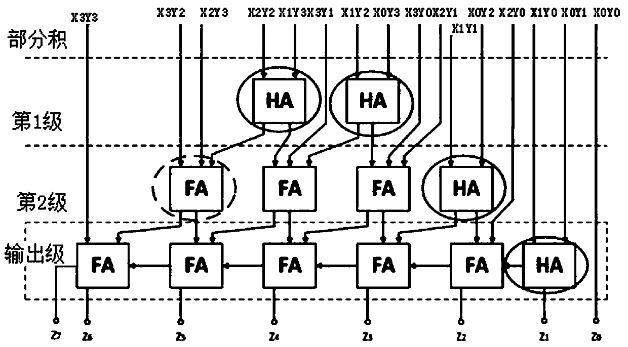
[0044] like Figure 4 As shown, it is a traditional wallace-tree digital multiplier. Taking 4 bits multiplied by 4 bits as an example, it is divided into the first level, the second level, and the output level. Each bit of the multiplier is obtained through an AND gate circuit; X0Y0 is the unit bit Z0; X0Y1 and X1Y0 are used as the input of the first CMOS half adder, the output sum is the tens bit Z1, and the output carry is used as the hundreds bit CMOS full adder of the output stage input; X0Y2 and X1Y1 are used as the input of the second CMOS half adder, and the output sum, X2Y0, and the output carry of the first CMOS half adder are collectively used as the input of the hundred-digit CMOS full adder, and the output sum is the hundred-digit Z2; X1Y2 and X0Y3 are used as the input of the third CMOS half adder; the output of the third CMOS half adder and, X3Y0, X2Y1 are jointly used as the input of the second-level thousand-bit CMOS full adder; the second-level thousand-bit CM...

Embodiment 2

[0046] On the basis of Embodiment 1, one or more of the first CMOS half adder, the second CMOS half adder, the third CMOS half adder, and the fourth CMOS half adder will be transformed into memristor arrays constitutes a half adder.

Embodiment 3

[0048] like figure 1 As shown, taking 4 bits multiplied by 4 bits as an example, it is divided into the first stage, the second stage, and the output stage. The partial product is used as the input, and the partial product is passed through each bit of the multiplier and the multiplicand through the AND gate circuit. Obtained; X0Y0 is the unit digit Z0; X0Y1 and X1Y0 are used as the input of the first half adder, the output sum is the tens digit Z1, and the output carry is used as the input of the hundred-digit CMOS full adder of the output stage; X0Y2 and X1Y1 are used as the second half adder The input of the device, the output sum, X2Y0, and the output carry of the first half adder are jointly used as the input of the hundred-digit CMOS full adder, and the output sum is the hundred-digit Z2; X1Y2 and X0Y3 are used as the input of the third half-adder; the third The output sum of the half adder, X3Y0, and X2Y1 are used as the input of the second-level thousand-bit CMOS full ...


PUM


Abstract

The invention discloses a memristor array which comprises metal wires and memristors. The metal wires are arranged in a cross manner. A memristor is arranged at the intersection of every two memristors; judging on-off of a metal wire according to the resistance value of the memristor; and forming an adder according to the resistance state of the memristor. The invention provides a memristor-CMOS (Complementary Metal Oxide Semiconductor) hybrid multiplication kernel circuit. One input of multiplication can be stored in a memristor network. According to the technical scheme, a CMOS circuit is used for storing the data, one part of operation is completed in the memory network, the other part of operation is completed through the CMOS circuit, so that half of frequent calling of the data is reduced, the power consumption of the CMOS circuit part is further reduced by reducing competition risks in the operation process, and the overall energy consumption can be greatly reduced.

Description

technical field [0001] The invention relates to the technical field of memristors, in particular to a half adder, full adder and multiplier based on a memristor array. Background technique [0002] Human society is at a turning point from an information society to an intelligent society, and artificial intelligence will fundamentally change our way of life. In recent years, with the successful application of big data and deep learning, computing intelligence in speech recognition, face recognition, knowledge search, intelligent driving and other fields has rapidly increased, and related research and applications have received unprecedented attention. One of the driving forces behind this is the ever-increasing computing power. In the past 40 years, with the advancement of integrated circuit technology and design, the processing power of processors has increased by nearly 100 billion times. However, with the increase in computing power comes a sharp increase in energy consum...

Claims


Application Information

Patent Timeline
Patent Type & Authority Applications(China)
IPC IPC(8): G06F7/502G06F7/523
CPCG06F7/502G06F7/523Y02D10/00G06F2207/4802G11C11/54G11C13/0007G06F7/5443G11C13/0002
Inventor 邹亮
Owner ZHUHAI FUDAN INNOVATION INST
Learn More