Deep ultraviolet LED structure and manufacturing method thereof

A technology of LED structure and manufacturing method, which is applied in the direction of semiconductor devices, electrical components, circuits, etc., can solve problems such as the reduction of external quantum efficiency of deep ultraviolet LEDs, and achieve the effect of improving external quantum efficiency

Active Publication Date: 2020-02-18
TSINGHUA UNIV
View PDF9 Cites 3 Cited by
  • Summary
  • Abstract
  • Description
  • Claims
  • Application Information

AI Technical Summary

Problems solved by technology

However, with the shortening of the emission wavelength, the external quantum efficiency (EQ

Method used


Image

  • Deep ultraviolet LED structure and manufacturing method thereof
  • Deep ultraviolet LED structure and manufacturing method thereof
  • Deep ultraviolet LED structure and manufacturing method thereof

Examples


no. 1 example

[0076] In a first exemplary embodiment of the present disclosure, a deep ultraviolet LED structure is provided.

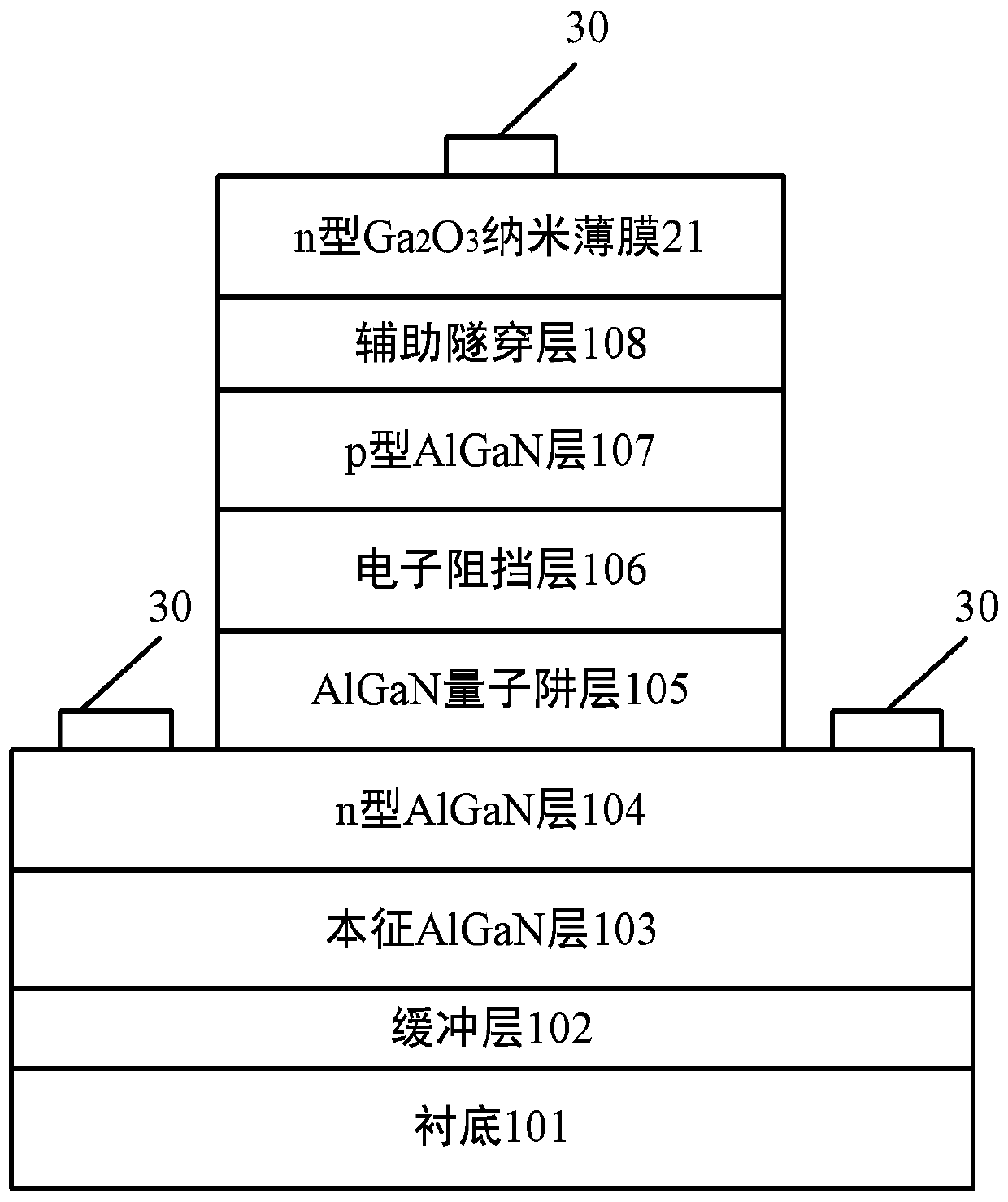
[0077] figure 1 It is a schematic diagram of a deep ultraviolet LED structure according to an embodiment of the present disclosure.

[0078] refer to figure 1 As shown, the deep ultraviolet LED structure of the present disclosure includes: a deep ultraviolet AlGaN epitaxial structure 10, including: a p-type AlGaN layer 107; an n-type Ga 2 o 3 Nano film 21, located on the upper surface of the deep ultraviolet AlGaN epitaxial structure 10; wherein, the n-type Ga 2 o 3 The nano film 21 forms a tunnel junction with the p-type AlGaN layer 107, serving as a surface electrode contact layer and a hole supply layer.

[0079] The n-type Ga 2 o 3 The nano film is on the order of hundreds of nanometers, such as in this embodiment, the n-type Ga 2 o 3 The thickness of the nano film 21 is 10 nanometers to 10 micrometers.

[0080] By using n-type Ga 2 o 3 The nano fil...

no. 2 example

[0107] In a second exemplary embodiment of the present disclosure, a method for fabricating a deep ultraviolet LED structure is provided.

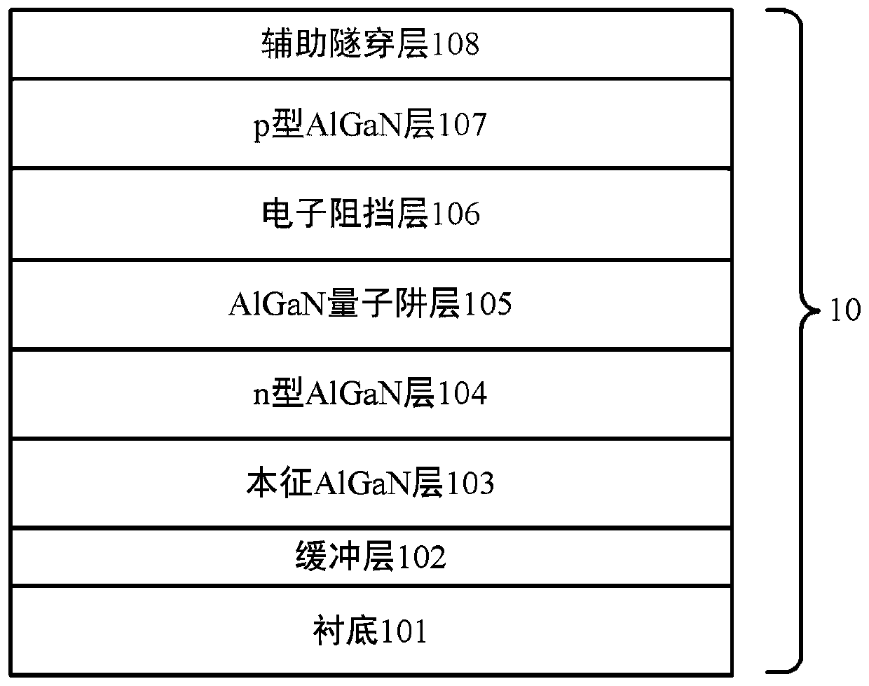
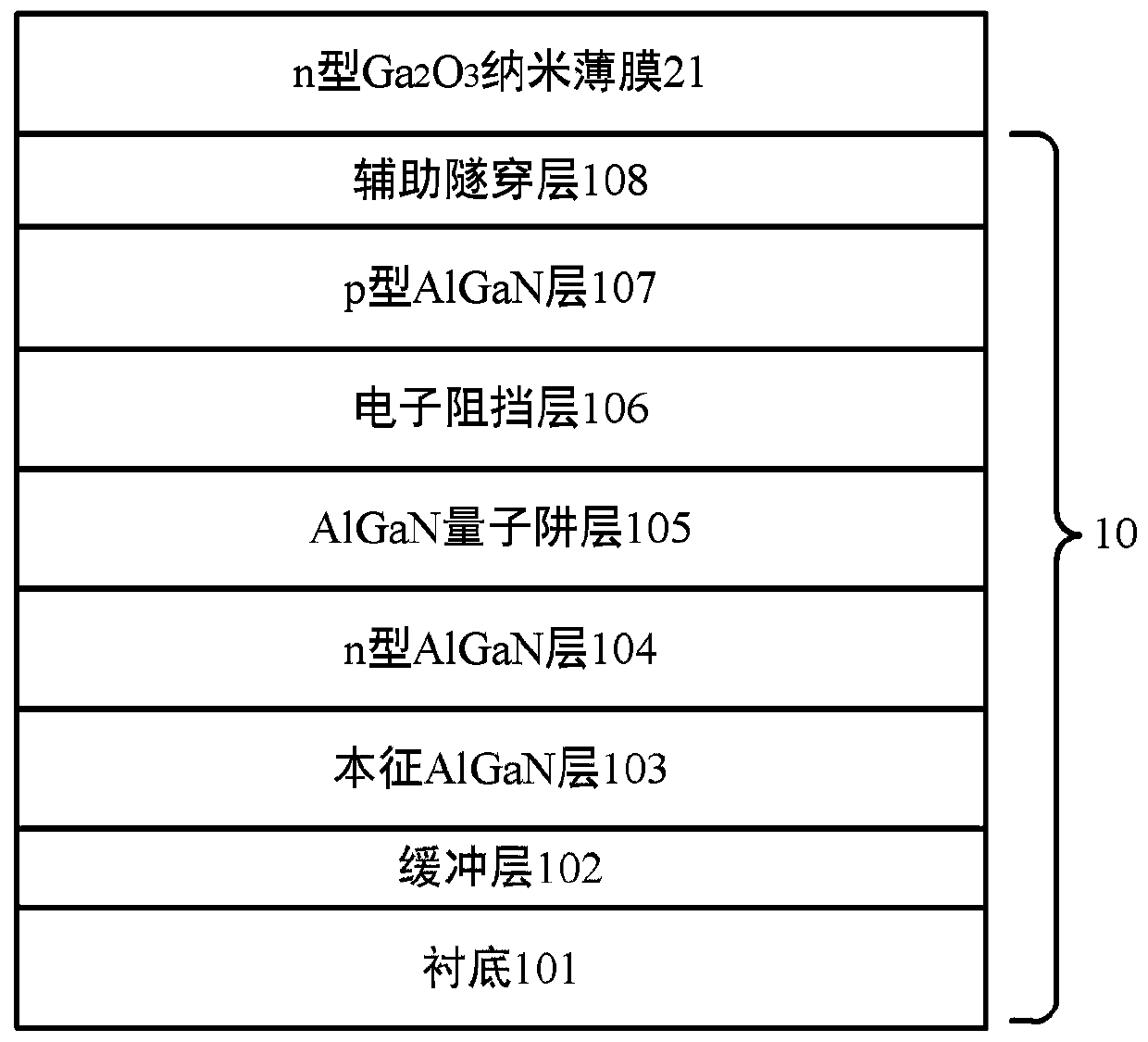
[0108] Figure 2-Figure 5 Each is a schematic diagram of the implementation process of each step corresponding to the manufacturing method of the deep ultraviolet LED structure shown in an embodiment of the present disclosure. in, figure 2 It is a schematic diagram of preparing a deep ultraviolet AlGaN epitaxial structure. image 3 n-type Ga 2 o 3 Schematic diagram of the transfer of nanofilms to the surface of deep-ultraviolet AlGaN epitaxial structures. Figure 4 for n-type Ga 2 o 3 Schematic illustration of the nanofilm etched down to the n-type AlGaN layer to make the mesa. Figure 5 Schematic diagram for forming electrodes on the mesas to form a deep-UV LED structure.

[0109] refer to Figure 2-Figure 5 As shown, the manufacturing method of the deep ultraviolet LED structure of the present disclosure includes:

[0110] Ste...


PUM

PropertyMeasurementUnit
Thicknessaaaaaaaaaa
Thicknessaaaaaaaaaa
Thicknessaaaaaaaaaa

Abstract

The invention discloses a deep ultraviolet LED structure and a manufacturing method thereof. The deep ultraviolet LED structure comprises a deep ultraviolet AlGaN epitaxial structure and an n-type Ga2O3 nano thin film, wherein the deep ultraviolet AlGaN epitaxial structure comprises a p-type AlGaN layer; the n-type Ga2O3 nano thin film is positioned on the upper surface of the deep ultraviolet AlGaN epitaxial structure; the n-type Ga2O3 nano thin film and the p-type AlGaN layer form a tunnel junction, and the tunnel junction is used as a surface electrode contact layer and a hole supply layer.The tunnel junction is formed by using the n-type Ga2O3 nano thin film and the p-type AlGaN layer, on one hand, the tunnel junction is used as a hole supply layer to improve the hole concentration, and on the other hand, the tunnel junction is used as a surface electrode contact layer and forms good ohmic contact with the surface electrode, so that the external quantum efficiency of the deep ultraviolet LED is improved, and meanwhile, the n-type Ga2O3 nano thin film has relatively high transmittance for light in a deep ultraviolet band and does not absorb light generated by the LED.

Description

technical field [0001] The disclosure belongs to the technical field of light emitting devices, and relates to a deep ultraviolet LED structure and a manufacturing method thereof. Background technique [0002] The light with an ultraviolet wavelength of 200-350 nanometers is called the deep ultraviolet band. Compared with the long-wave ultraviolet, the light source of the deep ultraviolet band is absorbed by the ozone layer when it reaches the surface of the earth, so its content in the environment is extremely weak. Due to its extremely short wavelength and extremely high photon energy, deep ultraviolet light can exert unique advantages in sterilization, purification, medical treatment, etc. [0003] Deep ultraviolet semiconductor light-emitting diode (LED) is a branch of LED. Compared with the traditional mercury lamp light source, it has many advantages, such as high efficiency, stability, energy saving, environmental protection and small size, etc., and can replace all c...

Claims


Application Information

Patent Timeline
IPC IPC(8): H01L33/32H01L33/14H01L33/06H01L33/04H01L33/00
CPCH01L33/0075H01L33/04H01L33/06H01L33/14H01L33/32
Inventor 汪莱刘洋郝智彪罗毅
Owner TSINGHUA UNIV
Why Eureka
Try Eureka