

Polishing pad and preparation method and application thereof
A polishing pad and polishing layer technology, which is applied in the direction of grinding/polishing equipment, manufacturing tools, metal processing equipment, etc., can solve the problems of increased wear rate and uneven wafer surface
- Summary
- Abstract
- Description
- Claims
- Application Information
AI Technical Summary
Problems solved by technology
Method used
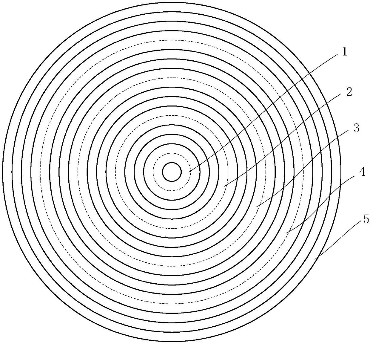
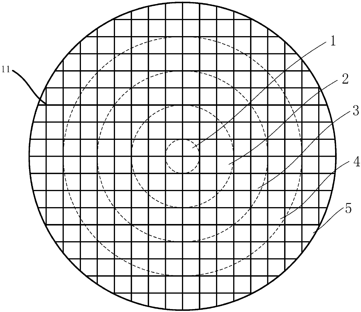
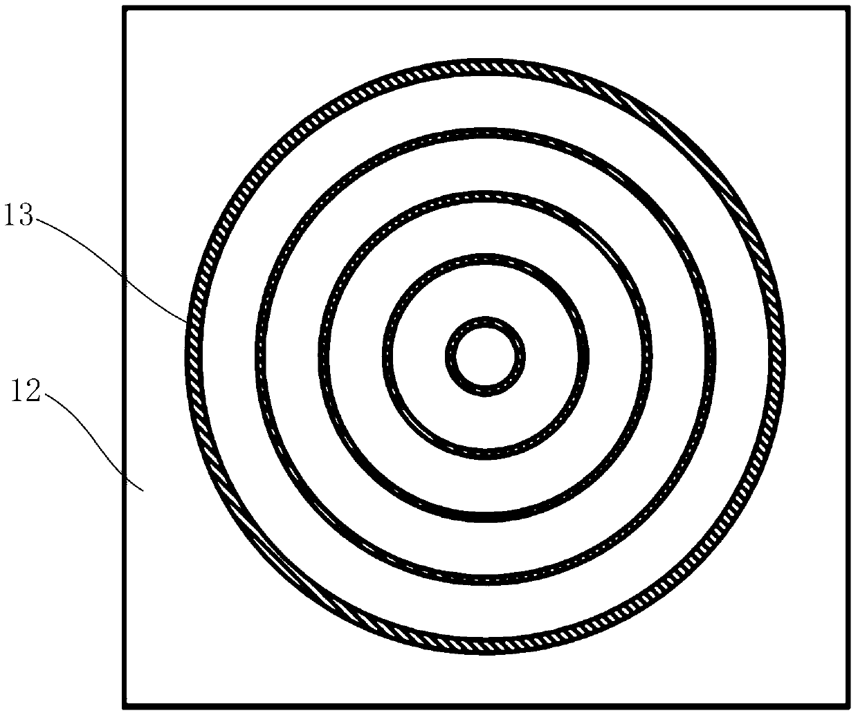
Image

Examples
Embodiment 1-6
[0079] Step (1): the treatment of the isocyanate-terminated polyurethane prepolymer (or prepolymer for short); the specific operations are as follows: 100 parts by mass of the isocyanate-terminated prepolymer obtained by the reaction of toluene diisocyanate and polytetrahydrofuran (The mass percentage of unreacted NCO group is 8.75-9.05%, the above-mentioned concrete numerical value of each embodiment is shown in Table 1 and Table 2) warming up to 80 ℃, degassing under vacuum (-0.095MPa) 2 hours; Then, add different The average diameter of the mass fraction (the content of the hollow microspheres is shown in Table 4) is the hollow microspheres of 20 microns, and the hollow microspheres are evenly dispersed in the prepolymer under stirring to obtain compositions with different microsphere contents; Compositions with different microsphere contents were degassed again under vacuum (-0.095MPa) for 2 hours, and then cooled to 50° C. to obtain prepolymers with different microsphere c...
PUM
| Property | Measurement | Unit |
|---|---|---|
| Diameter | aaaaa | aaaaa |
| Diameter | aaaaa | aaaaa |
| Thickness | aaaaa | aaaaa |
Abstract
Description
Claims
Application Information