A display substrate, its preparation method, and a display device

A technology of display substrate and non-display area, which is applied in semiconductor/solid-state device manufacturing, semiconductor devices, electrical components, etc., can solve problems such as poor electrical conductivity and large driving voltage gap, achieve simple preparation methods, solve voltage drop, improve Effect of resistance value

Active Publication Date: 2022-06-24
BOE TECH GRP CO LTD +1
View PDF0 Cites 0 Cited by
  • Summary
  • Abstract
  • Description
  • Claims
  • Application Information

AI Technical Summary

Problems solved by technology

The top emission needs to take into account the light transmittance, so a thinner transparent cathode is required, which will lead to poor conductivity. When the screen size is large, the center area of ​​the screen is far away from the electrode area, and the long-distance current transmission increases the driving voltage. Larger, it is easy to cause a large gap between the driving voltage of the OLED device in the center area of ​​the screen and the edge area, that is, the problem of voltage drop (IR Drop)

Method used


Image

  • A display substrate, its preparation method, and a display device
  • A display substrate, its preparation method, and a display device
  • A display substrate, its preparation method, and a display device

Examples


Embodiment Construction

[0030] The technical solutions in the embodiments of the present invention will be clearly and completely described below with reference to the accompanying drawings in the embodiments of the present invention. Obviously, the described embodiments are only a part of the embodiments of the present invention, but not all of the embodiments. Based on the embodiments of the present invention, all other embodiments obtained by those of ordinary skill in the art without creative efforts shall fall within the protection scope of the present invention.

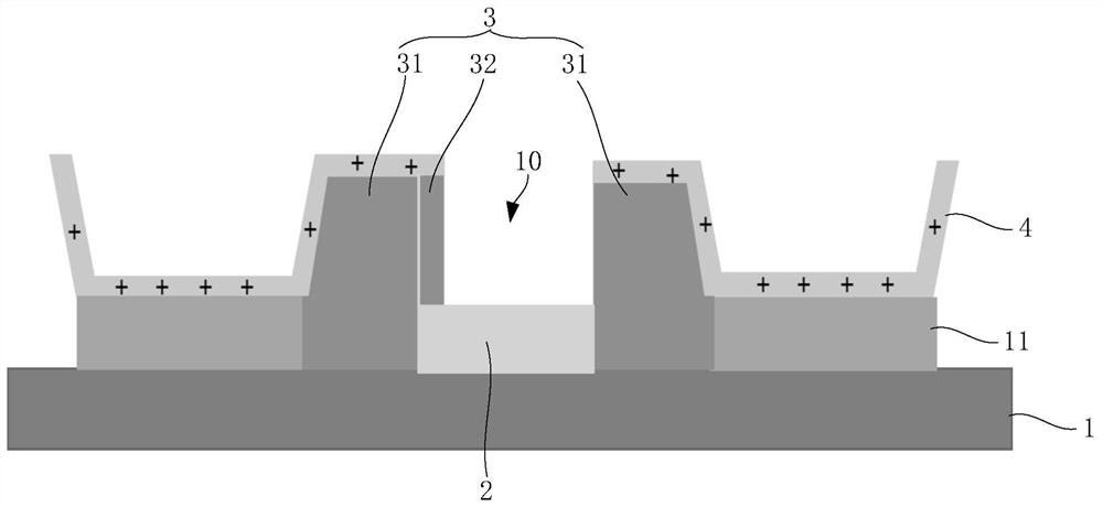
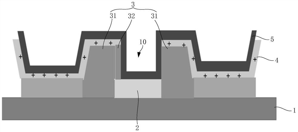
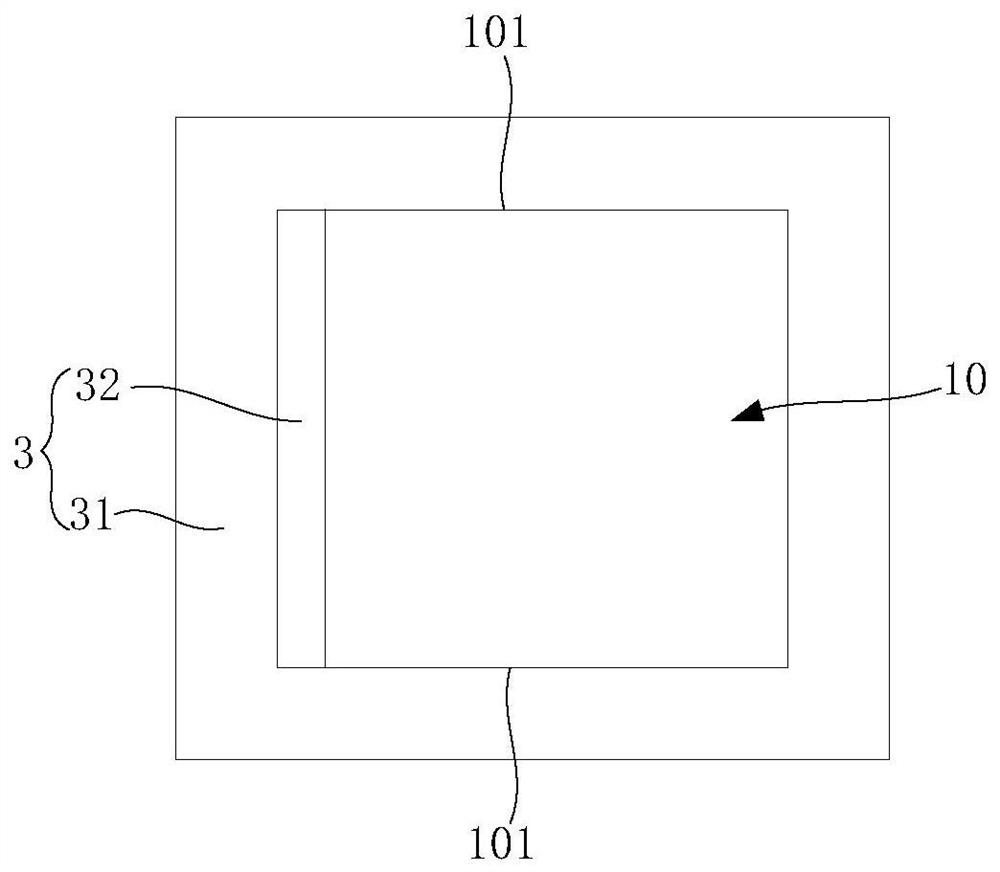
[0031] like Figure 1 to Figure 5 As shown, an embodiment of the present invention provides a display substrate, including a driving backplane 1, and an auxiliary electrode 2, a pixel defining structure 3, a light-emitting functional layer 4 and a first electrode layer 5 located on the driving backplane 1; in:

[0032] The pixel defining structure 3 and the auxiliary electrode 2 are located in the non-display area;

[0033] The pixe...


PUM

PropertyMeasurementUnit
depthaaaaaaaaaa
widthaaaaaaaaaa

Abstract

The invention relates to the field of display technology, and discloses a display substrate, a preparation method thereof, and a display device. The display substrate includes a driving backplane, auxiliary electrodes located on the driving backplane, a pixel defining structure, a light-emitting functional layer, and a first electrode layer; the auxiliary electrodes and the pixel defining structure are located in the non-display area; the pixel defining structure surrounds the auxiliary electrodes, and is connected with the The auxiliary electrode surrounds a groove, and the auxiliary electrode is configured as the bottom wall of the groove; at least part of the side walls of the groove have electromagnetic properties, and are configured to use electromagnetic force to make it difficult for the charged evaporation material to deposit on the bottom wall of the groove ; The material of the light-emitting functional layer is configured as a charged evaporation material; the first electrode layer covers the groove and is in direct contact with the bottom wall of the groove. The above-mentioned display substrate is provided with an auxiliary electrode, which can solve the voltage drop problem of the first electrode layer, and the display substrate has a simple structure, and the contact connection between the first electrode layer and the auxiliary electrode can be realized through simple process steps, and the preparation method is simple.

Description

technical field [0001] The present invention relates to the field of display technology, in particular to a display substrate, a preparation method thereof, and a display device. Background technique [0002] Existing OLED devices are divided into two types: bottom emission and top emission. Since top emission can obtain a larger aperture ratio, it has become a research hotspot in recent years. Top emission needs to take into account the light transmittance, so a thinner transparent cathode is required, which will lead to poor conductivity. When the screen size is large, the central area of ​​the screen is far away from the electrode area, and the long-distance current transmission increases the driving voltage. If it is larger, it is easy to cause a large difference between the driving voltage of the OLED device in the central area of ​​the screen and the edge area of ​​the screen, that is, the problem of voltage drop (IR Drop). Therefore, it is necessary to improve the ca...

Claims


Application Information

Patent Timeline
Patent Type & Authority Patents(China)
IPC IPC(8): H01L27/32H01L51/52H01L51/56H01L51/00
CPCH10K59/122H10K71/16H10K50/824H10K71/00
Inventor 屈丽桃殷卫东徐志伟屈玉恩
Owner BOE TECH GRP CO LTD
Why Eureka
Try Eureka