Array substrate, display panel and display device

A technology for array substrates and display panels, applied in projection devices, printing devices, static indicators, etc., can solve problems affecting the arrangement of wires on array substrates and the performance of electronic devices, etc., to achieve compact arrangement and reduce wiring area Effect

Pending Publication Date: 2020-02-28
HONG FU JIN PRECISION IND (SHENZHEN) CO LTD +1
View PDF4 Cites 3 Cited by
  • Summary
  • Abstract
  • Description
  • Claims
  • Application Information

AI Technical Summary

Problems solved by technology

[0003] Taking an array substrate including multiple wires in an electronic device as an example, the array substrate needs to be provided with a camera hole area that exposes the camera module. However, the camera hole area will affect the arrangement of the wires on the array substrate, and even affect the performance of the electronic device.

Method used


Image

  • Array substrate, display panel and display device
  • Array substrate, display panel and display device
  • Array substrate, display panel and display device

Examples


Embodiment Construction

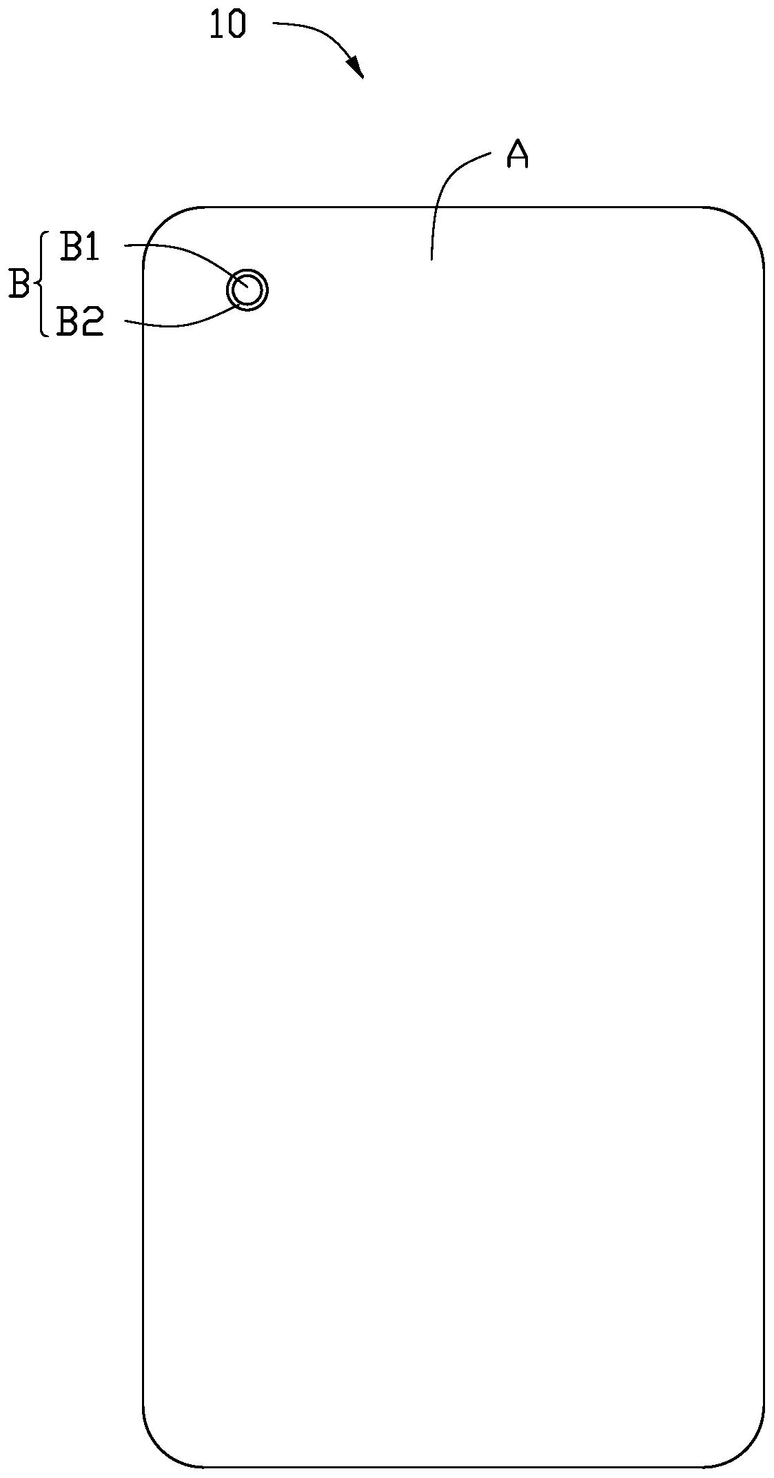
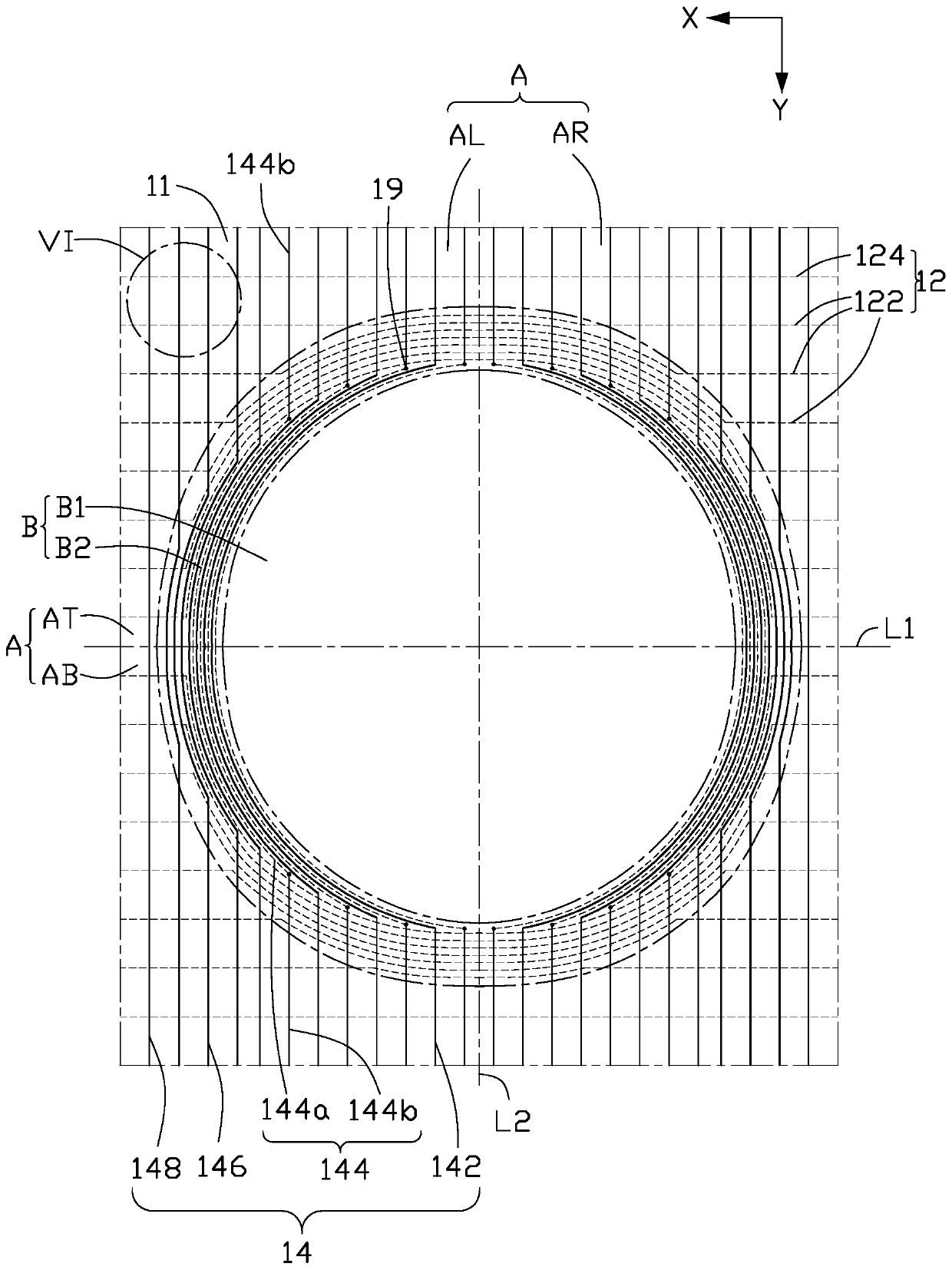
[0068] Such as figure 1 As shown, the array substrate 10 defines a display area A and a camera hole area B surrounded by the display area A. As shown in FIG. The camera hole area B defines a hollow area B1 and a routing area B2 surrounding the hollow area B1. The camera hole area B is a light-transmitting area. The camera hole area B and the hollow area B1 are roughly circular, and the wiring area B2 is a ring. In other embodiments, the camera hole area B can also have other shapes. For example, oval, polygon, etc.

[0069] Such as figure 2 As shown, the routing area B2 has a first axis of symmetry L1 and a second axis of symmetry L2. Along the first direction X, the wiring area B2 is distributed axisymmetrically with respect to the second axis of symmetry L2. Along the second direction Y, the wiring area B2 is distributed axisymmetrically with respect to the first axis of symmetry L1. The second direction Y intersects the first direction X. Along the first direction ...


PUM


Abstract

The invention provides an array substrate, a display panel applying the array substrate and a display device. The array substrate is provided with a display area and a camera hole area surrounded by the display area. The camera hole area is provided with a hollow area and a wiring area surrounding the hollow area. The array substrate comprises a plurality of first data lines and a plurality of second data lines which are sequentially and alternately arranged in the first direction. Each first data line and each second data line bypass the hollow area, span the wiring area and extend in the second direction in the display area. Each second data line comprises an auxiliary data line located in the wiring area and a data line lead electrically connected with the auxiliary data line and extending in the second direction. The auxiliary data line is defined by a first conductive layer, and the first data line and the data line lead are defined by a second conductive layer different from thefirst conductive layer.

Description

technical field [0001] The present invention relates to the field of display technology, and in particular to an array substrate, a display panel using the array substrate, and a display device using the display panel. Background technique [0002] Electronic devices, such as mobile phones, tablet computers, etc., often need to be combined with components with other functions as users have increasing demands for diversified functions. Among them, electronic devices combined with camera modules have been widely produced and applied. [0003] Taking an array substrate including multiple wires in an electronic device as an example, the array substrate needs to be provided with a camera hole area that exposes the camera module. However, the camera hole area will affect the arrangement of the wires on the array substrate, and even affect the performance of the electronic device. . Contents of the invention [0004] One aspect of the present invention provides an array substra...

Claims


Application Information

Patent Timeline
Patent Type & Authority Applications(China)
IPC IPC(8): G02F1/1362G02F1/1368G03B29/00H01L27/12
CPCG02F1/136286G02F1/1368G03B29/00H01L27/124G02F1/13312G09G2300/0426G03B30/00H04M1/0264H04M1/0266G02F1/136222G02F1/136227G02F2201/123G09G3/3677G09G3/3688
Inventor 欧阳祥睿陈维成
Owner HONG FU JIN PRECISION IND (SHENZHEN) CO LTD
Why Eureka
Try Eureka