Supercharge Your Innovation With Domain-Expert AI Agents!

Semiconductor device, pixel circuit, display panel and display device

A technology for display panels and display devices, applied in the fields of display panels and display devices, pixel circuits, and semiconductor devices, can solve the problems of poor heat resistance, abnormal display, threshold voltage shift of oxide semiconductor transistors, etc., and achieve improved stability. and reliability, the effect of improving stability and reliability

Active Publication Date: 2022-07-29
BOE TECH GRP CO LTD +1
View PDF0 Cites 0 Cited by
  • Summary
  • Abstract
  • Description
  • Claims
  • Application Information

AI Technical Summary

Problems solved by technology

However, the active layer of the oxide semiconductor transistor is an oxide semiconductor material, and the heat resistance of the oxide semiconductor material is poor. Oxygen in the active layer is easy to escape at high temperature, causing the threshold voltage of the oxide semiconductor transistor to drift, which in turn leads to display The device fails, or the display is abnormal

Method used


Image

  • Semiconductor device, pixel circuit, display panel and display device
  • Semiconductor device, pixel circuit, display panel and display device
  • Semiconductor device, pixel circuit, display panel and display device

Examples


Embodiment Construction

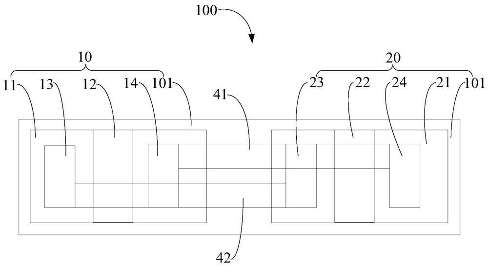
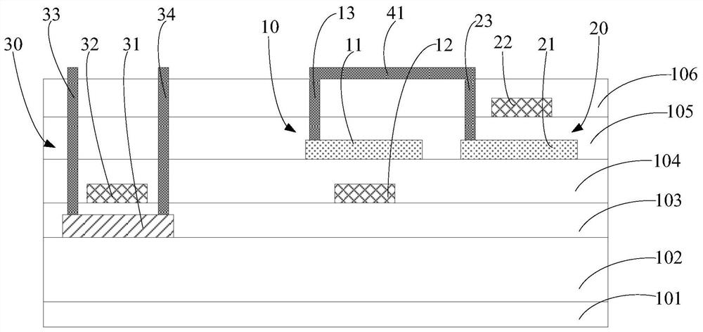
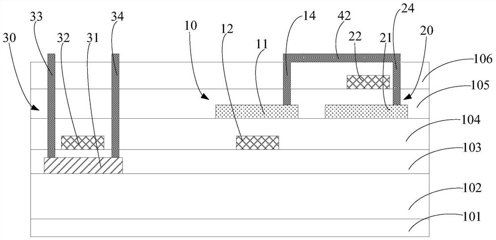
[0028] Exemplary embodiments will be described in detail herein, examples of which are illustrated in the accompanying drawings. Where the following description refers to the drawings, the same numerals in different drawings refer to the same or similar elements unless otherwise indicated. The implementations described in the illustrative examples below are not intended to represent all implementations consistent with this application. Rather, they are merely examples of means consistent with some aspects of the present application as recited in the appended claims.

[0029] The terminology used in this application is for the purpose of describing particular embodiments only and is not intended to limit the application. Unless otherwise defined, technical or scientific terms used in this application shall have the ordinary meaning as understood by those of ordinary skill in the art to which this application belongs. Words like "a" or "an" used in the specification and claims...


PUM


Abstract

The present application provides a semiconductor device, a pixel circuit, a display panel and a display device. The semiconductor device includes N first thin film transistors, where N is a natural number greater than or equal to 2. The first thin film transistor includes a substrate, a first active layer, a first gate electrode, a first source electrode and a first drain electrode, the first active layer, the first gate electrode, the first The source electrode and the first drain electrode are formed on the substrate; the material of the first active layer is an oxide semiconductor material; the first gate electrode and the first active layer are insulated from each other, so The first source electrode and the first drain electrode are respectively electrically connected to the first active layer. The first source electrodes of the N first thin film transistors are electrically connected, and the first drain electrodes of the N first thin film transistors are electrically connected.

Description

technical field [0001] The present application relates to the field of semiconductor technology, and in particular, to a semiconductor device, a pixel circuit, a display panel and a display device. Background technique [0002] In recent years, display devices based on OLED (Organic Light Emitting Diode, Organic Light Emitting Diode) have become popular display products at home and abroad due to their advantages of self-luminescence, wide viewing angle, high luminous efficiency, wide color gamut, low operating voltage and thin panel. . [0003] The driving mode of the OLED display device is generally active driving, that is, the pixels of the display device are driven by the pixel circuit. A switching transistor in a general pixel circuit adopts an oxide semiconductor transistor. However, the active layer of the oxide semiconductor transistor is made of oxide semiconductor material, and the oxide semiconductor material has poor heat resistance, and oxygen in the active lay...

Claims


Application Information

Patent Timeline
Patent Type & Authority Patents(China)
IPC IPC(8): H01L27/32
CPCH10K59/123H10K59/124H10K59/1213H10K59/12H10K59/1201
Inventor 黄鹏詹裕程高涛
Owner BOE TECH GRP CO LTD
Features
  • R&D
  • Intellectual Property
  • Life Sciences
  • Materials
  • Tech Scout
  • Unparalleled Data Quality
  • Higher Quality Content
  • 60% Fewer Hallucinations
Learn More