

Display panel packaging structure, display panel and display device
A packaging structure and display panel technology, which is applied in the fields of optics, instruments, electrical components, etc., can solve problems such as cracks in the packaging structure, and achieve good packaging effect, stable display effect and long service life
- Summary
- Abstract
- Description
- Claims
- Application Information
AI Technical Summary
Problems solved by technology
Method used
Image

Examples
Embodiment 1
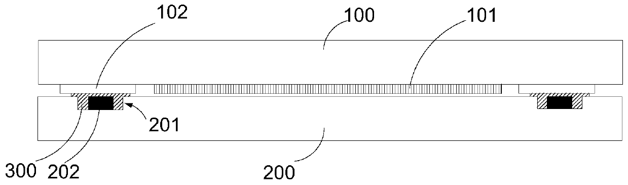
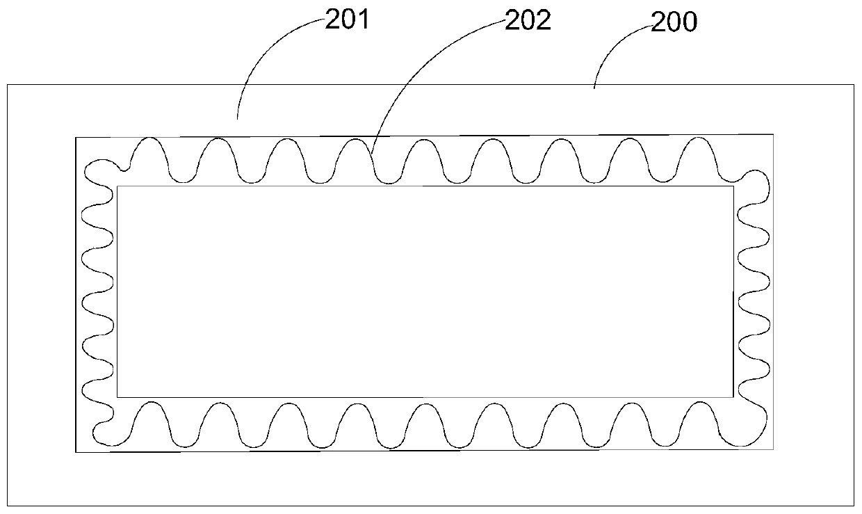
[0059] as image 3 The structure shown is taken as an example. An annular groove 201 with a width of 0.5 mm and a depth of 0.2 mm is provided in the middle area of the preset coating position of glass glue on the package cover 200; 0.4mm and 0.25mm high lead-bismuth alloy S-shaped bent ring-shaped metal strip, coated with glass glue at the position of the groove 201, the width of the glass glue is 0.7mm; heat the package cover plate 200 at 100°C for 1 hour, bake and package Cover plate 200, remove the encapsulant 300 solvent; make a 1 μm wide SiNx protective layer 102 on the OLED substrate 100 corresponding to the glass glue area, press the encapsulation cover plate 200 and the OLED substrate 100, make the metal strip contact with the substrate 100, and the glass glue area is laser cured, complete image 3 The package structure shown.
Embodiment 2
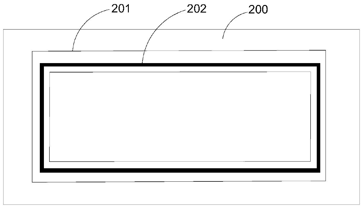
[0061] as Figure 5 The structure shown is taken as an example. An annular groove 201 with a width of 0.5mm and a depth of 0.2mm is provided in the middle area of the preset coating position of glass glue on the packaging cover plate 200; mm, 0.4mm high lead-bismuth alloy spiral annular metal strip, coated with glass glue at the position of groove 201, the width of glass glue is 0.7mm; heat the cover plate at 100°C for 1h, bake the package cover plate 200, remove Encapsulation glue 300 solvent; make a 1 μm wide SiNx protective layer 102 on the OLED substrate 100 corresponding to the glass glue area, press the packaging cover plate 200 and the OLED substrate 100, make the spiral metal strip contact with the substrate 100 and compress until it is no longer deformed, Laser curing the glass glue area, complete as Figure 5 The package structure shown.
[0062] It should be noted that the exemplary packaging structure described above can be used not only for OLED display panels...
PUM
 Abstract
Description
Claims
Application Information