Dielectric capacitor

A technology of dielectric capacitance and capacitance layer, which is applied in the direction of capacitors, circuits, electrical components, etc., can solve the problems of restricting the increase of the capacitance value per unit area and the inability to increase the capacitance value of the capacitance per unit area, and achieve the effect of increasing the capacitance value per unit area

Inactive Publication Date: 2020-03-03
CSMC TECH FAB2 CO LTD
View PDF4 Cites 0 Cited by
  • Summary
  • Abstract
  • Description
  • Claims
  • Application Information

AI Technical Summary

Problems solved by technology

Therefore, the arrangement of the comb teeth perpendicular to each other cannot increase the capacitance value per unit area of ​​the capacitor.
And when making capacitors, it is necessary to reserve the position on the side of the comb to set the through hole 12, which further restricts the improvement of the capacitance value per unit area

Method used


Image

  • Dielectric capacitor
  • Dielectric capacitor
  • Dielectric capacitor

Examples


no. 1 example

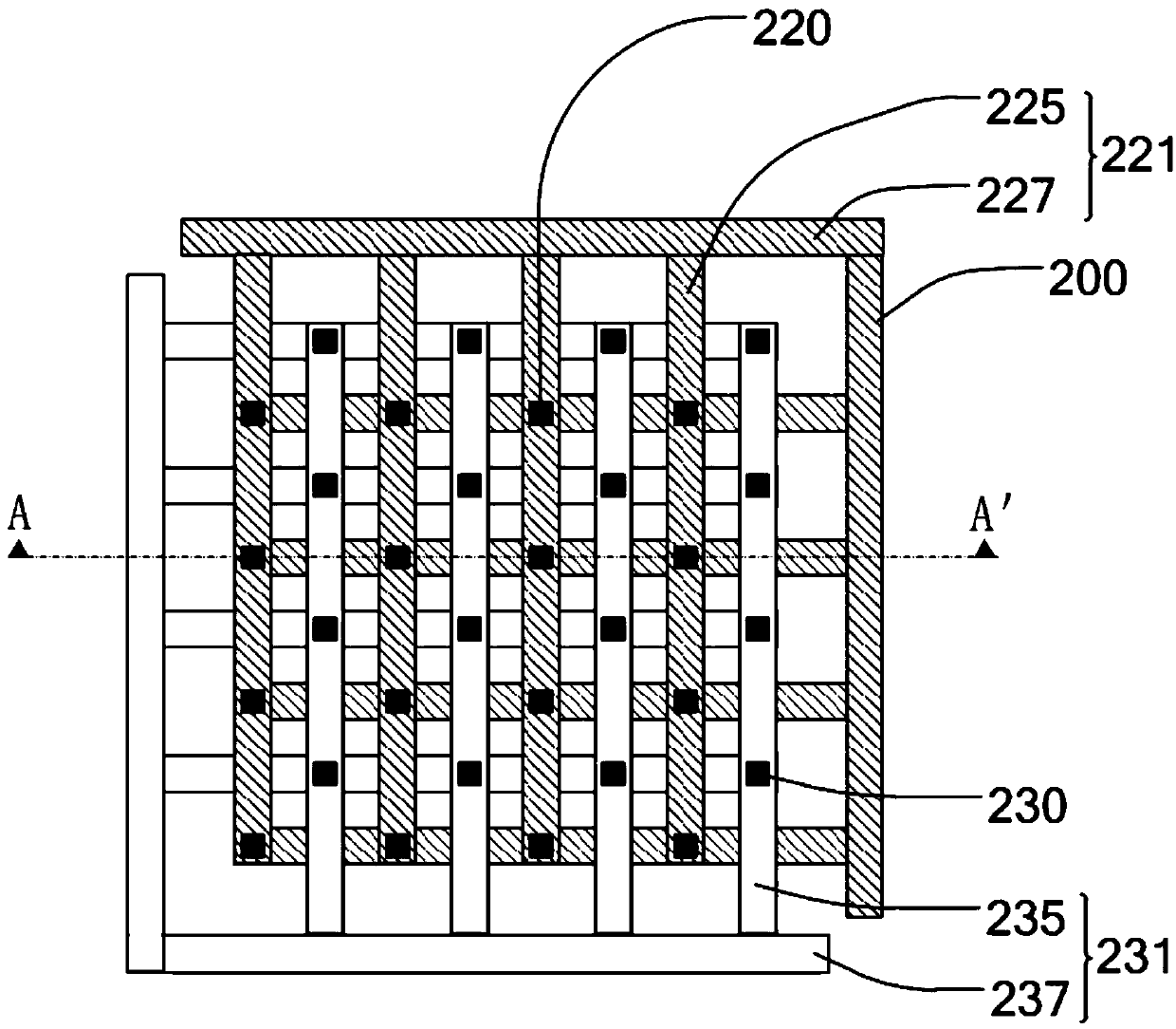
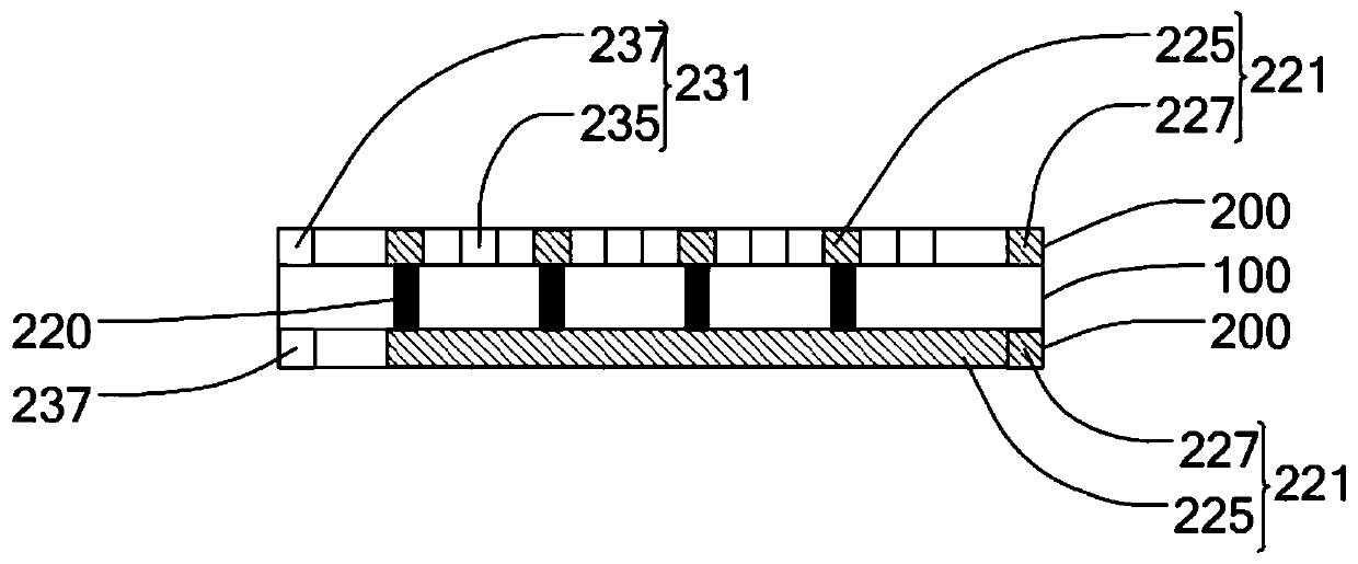
[0032] figure 2 is a top view of the dielectric capacitor of the first embodiment, image 3 for along figure 2 The side sectional view of the line A-A' in the middle.

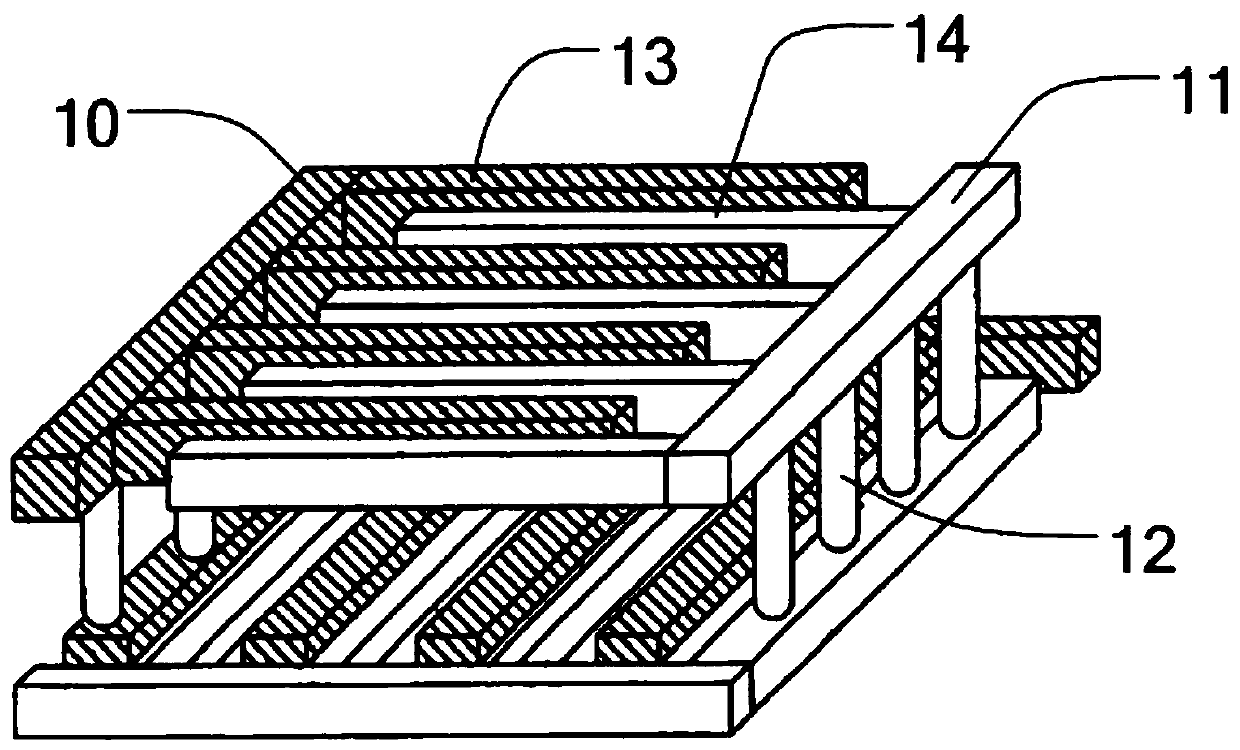
[0033] In this example, see figure 2 As shown, a dielectric capacitor includes at least two capacitor layers 200, each capacitor layer 200 has a positive electrode 221 and a negative electrode 231, and a dielectric material is filled between the positive electrode 221 and the negative electrode 231 (the dielectric material is in the figure 1 not shown). Positive electrode 221 is made up of a first part 227 and several intervals in parallel and is respectively joined to the second part 225 on one side of this first part 227, and negative electrode 231 is made up of a first part 237 and several intervals in parallel and is joined respectively. On one side of the first part 237 the second part 235 is formed. And in each capacitive layer 200, the second part 225 of the positive electrode 221 and the second ...

no. 2 example

[0039] In this example, see Figure 5 As shown, the capacitor layer is divided into a plurality of odd-number capacitor layers 300 and a number of even-number capacitor layers 400 that are alternately stacked. The alternate stacking method is specifically that an even-number capacitor layer 400 is arranged between every two odd-number capacitor layers 300, and a dielectric layer 500 is arranged between adjacent odd-number capacitor layers 300 and even-number capacitor layers 400. . Also, in order to clearly show the structure and arrangement of comb electrodes and vias, Figure 4 , Figure 5 , Image 6 with Figure 7 The dielectric materials filled in the odd-number capacitor layer 300 , the even-number capacitor layer 400 and the dielectric layer 500 are not shown in the figures.

[0040] see Image 6 The top view of the odd-numbered capacitor layer of the dielectric capacitor, the comb-tooth portion 325 of the positive electrode 321 in the odd-numbered capacitor layer ...


PUM


Abstract

The invention relates to a dielectric capacitor. In comparison with the traditional structure, the second parts of the positive electrodes in the two adjacent capacitor layers are vertically conductedthrough positive electrode through holes, and the second parts of the negative electrodes in the two adjacent capacitor layers are vertically conducted through negative electrode through holes. An extra capacitor connected with an existing multilayer parallel capacitor in parallel can be formed between the positive electrode through holes and the negative electrode through holes which are adjacent in pairs, and the capacitance value per unit area is greatly improved. In addition, a through hole does not need to be additionally formed to connect the first parts of the same-polarity electrodesin the two adjacent capacitor layers, so that the capacitance value per unit area can be further improved.

Description

technical field [0001] The invention relates to the technical field of semiconductor preparation, in particular to a dielectric capacitor used in integrated circuits. Background technique [0002] In the semiconductor manufacturing process, the dielectric capacitor is widely used in the integrated circuit design of the chip. With the rapid development of integrated circuit design and manufacturing technology of chips, while the critical dimensions of chips are continuously reduced and the integration of devices is getting higher and higher, the requirements of integrated circuit design for chip performance, device reliability and manufacturing cost are also increasing. Higher and higher. Among them, the dielectric capacitor is an important device of the integrated circuit. Whether the manufacturing cost of the dielectric capacitor can be effectively reduced and the capacitance density per unit area can be increased is of great significance for improving the chip integration...

Claims


Application Information

Patent Timeline
IPC IPC(8): H01L23/64H01L27/08
CPCH01L27/0805H01L28/40
Inventor 刘新新何小东孙晓峰
Owner CSMC TECH FAB2 CO LTD
Why Eureka
Try Eureka