Forming method for semiconductor device

A semiconductor and device technology, applied in the field of semiconductor device formation, can solve problems such as mutual interference, affecting device performance and stability, and achieve the effect of avoiding mutual interference, improving performance and stability, and being easy to receive.

Active Publication Date: 2020-03-10
CHANGXIN MEMORY TECH INC
View PDF10 Cites 1 Cited by
  • Summary
  • Abstract
  • Description
  • Claims
  • Application Information

AI Technical Summary

Problems solved by technology

[0003] The purpose of the present invention is to provide a method for forming a semiconductor device to solve the problem

Method used


Image

  • Forming method for semiconductor device
  • Forming method for semiconductor device
  • Forming method for semiconductor device

Examples


Example Embodiment

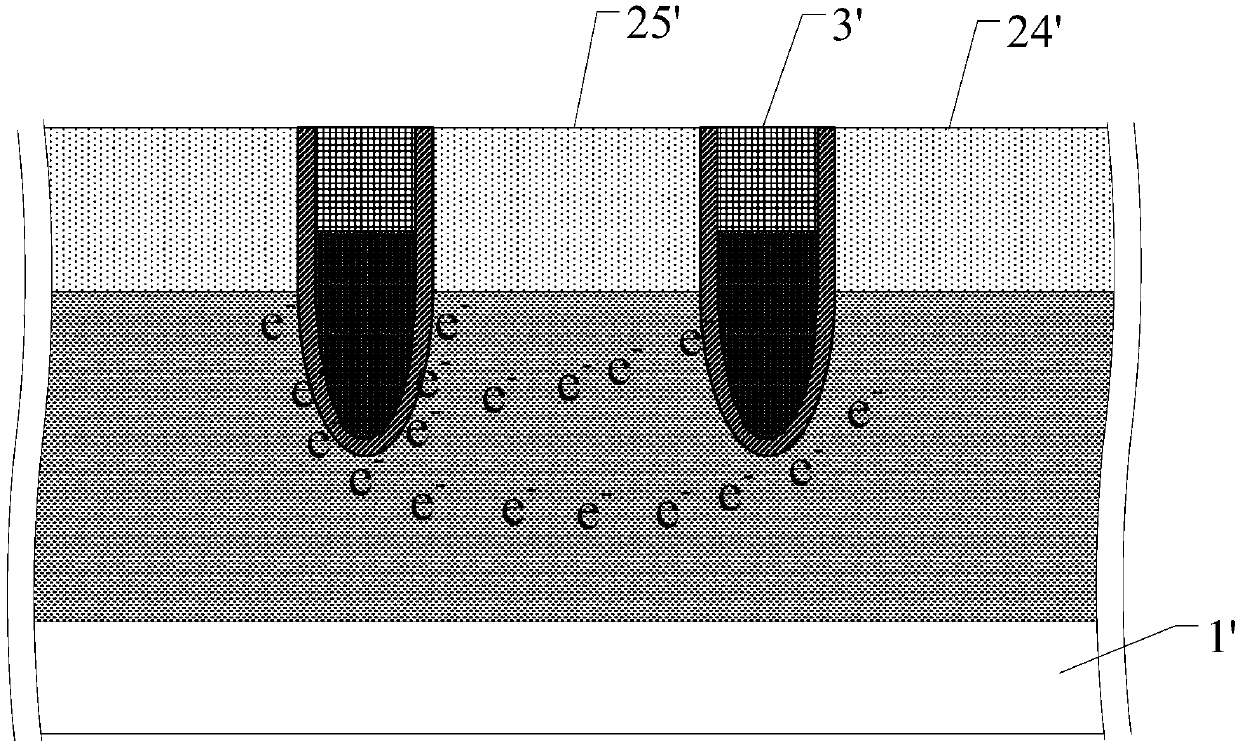
[0035] There is a semiconductor device such as figure 1 As shown, it includes a substrate 1' and two gate structures 3', a drain region 25' and a plurality of source regions 24' are formed in the substrate 1, and the source regions 24' conform to the active region The extension direction is arranged on both sides of the drain region 25', and each gate structure 3' is formed in the substrate between the drain region 25' and the source region 24' to form an access transistors, the adjacent access transistors in the same active region share the drain region 25', and the drain region 25' and the source region 24' extend downward from the surface of the substrate 1' to the same depth , forming a symmetrical structure. It can be understood that, when this semiconductor device is in use, the part of the substrate 1' along the bottom of the gate structure 3' constitutes a channel region, and when an access transistor is turned on, its source region 24' When the electrons migrate to ...


PUM


Abstract

The invention provides a forming method for a semiconductor device. Firstly, a plurality of gate structures are formed in a substrate; each gate structure is formed between a drain region and a sourceregion, and a plurality of access transistors are formed; the adjacent access transistors in the same active region share the drain region; twice ion implantation are carried out so as to enable thebottom of the drain region to sink to each source region; when the access transistors are used, electrons flow to the drain regions from the source regions, and the bottoms of the drain regions more sink to the source regions, so that the drain regions receive the electrons more easily, mutual interference caused by stray current formed between the two access transistors is avoided, and the performance and stability of the device are improved.

Description

technical field [0001] The invention relates to the field of semiconductor manufacturing, in particular to a method for forming a semiconductor device. Background technique [0002] At present, the existing DRAM chip usually includes several access transistors. In order to reduce the area of ​​the DRAM chip to achieve the highest integration level, a trench-type transistor structure is usually used, and can be placed in an active region Fabricate two access transistors with a shared drain to further reduce the area. It is conceivable that the distance between the two access transistors is very close (about 20nm), which makes it easy to generate stray current when the access transistor is in use, causing crosstalk between the two access transistors and affecting the device. performance and stability. Contents of the invention [0003] The object of the present invention is to provide a method for forming a semiconductor device to solve the problem that two transistors sha...

Claims


Application Information

Patent Timeline
IPC IPC(8): H01L21/8242H01L27/108
CPCH10B12/00H10B12/01
Inventor 不公告发明人
Owner CHANGXIN MEMORY TECH INC
Why Eureka
Try Eureka