Semiconductor laser and preparation method thereof

A semiconductor and laser technology, applied in semiconductor lasers, semiconductor laser devices, lasers, etc., can solve the problems of low saturated output power, low yield, and inability to achieve high power

Active Publication Date: 2020-03-17
CHANGCHUN INST OF OPTICS FINE MECHANICS & PHYSICS CHINESE ACAD OF SCI
View PDF10 Cites 13 Cited by
  • Summary
  • Abstract
  • Description
  • Claims
  • Application Information

AI Technical Summary

Problems solved by technology

However, the preparation of the grating structure of the distributed feedback semiconductor laser (DFB) generally requires technologies such as secondary epitaxy or electron beam lithography, resulting in high chip manufacturing costs and low yields; ridge DBR lasers generally use ridges (width 2- 5 micron) waveguide structure suppresses high-order side modes and reduces laser linewidth, which leads to low saturated output power and cannot achieve high-power narrow-linewidth laser

Method used


Image

  • Semiconductor laser and preparation method thereof
  • Semiconductor laser and preparation method thereof
  • Semiconductor laser and preparation method thereof

Examples


Embodiment Construction

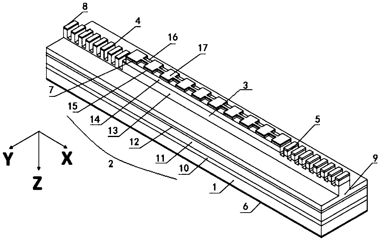
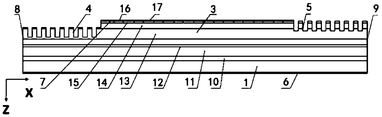
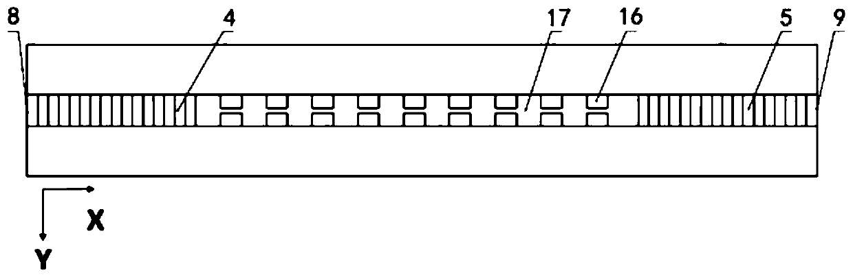
[0046]The core of the present invention is to provide a semiconductor laser. In the prior art, narrow linewidth semiconductor lasers usually include distributed feedback (DFB) lasers and ridge DBR lasers, although great progress has been made in increasing output power and reducing spectral linewidth. However, the preparation of the grating structure of the distributed feedback semiconductor laser (DFB) generally requires technologies such as secondary epitaxy or electron beam lithography, resulting in high chip manufacturing costs and low yields; ridge DBR lasers generally use ridges (width 2- 5 micron) waveguide structure suppresses high-order side modes and reduces the laser linewidth, which leads to low saturated output power and cannot achieve high-power narrow-linewidth lasers.

[0047] In the semiconductor laser provided by the present invention, a narrow strip waveguide is etched on the surface of the transmission layer facing away from the substrate, a first Bragg gra...


PUM


Abstract

The invention discloses a semiconductor laser. A narrow strip-shaped waveguide is etched on the surface of one side, back to a substrate, of a transmission layer, a first Bragg grating is arranged along one end of the axis of the narrow strip-shaped waveguide, and a second Bragg grating is arranged at the other end of the axis of the narrow-strip-shaped waveguide. The refractive index of a convexpart in the first Bragg grating is smaller than that of a convex part in the second Bragg grating, the refractive index of a concave part in the first Bragg grating is smaller than that of a concave part in the second Bragg grating, and the reflection spectrum of the first Bragg grating and the reflection spectrum of the second Bragg grating overlap at a preset wavelength. The laser outputted by the semiconductor laser can obtain the reflection spectrum superposition similar to a vernier effect, the ultra-narrow reflection spectrum is achieved, the spectral line width of a device is reduced, and the high-power narrow-line-width laser is achieved. The invention also provides a preparation method which also has the above beneficial effects.

Description

technical field [0001] The invention relates to the technical field of semiconductor lasers, in particular to a semiconductor laser and a method for preparing the semiconductor laser. Background technique [0002] Semiconductor lasers are lasers that use semiconductor materials as gain media, and have the advantages of small size, high efficiency, long life, and easy integration. Narrow linewidth semiconductor laser has the advantages of narrow spectral linewidth and high output power. It can be used as an ideal pump source for doped optical fibers and alkali metal atomic gases with narrow absorption spectrum characteristics. It is used in optical communication, ocean detection, space communication, atomic clock pumping Pu and other aspects have broad application prospects. [0003] Existing single-chip narrow-linewidth semiconductor lasers usually include distributed feedback (DFB) lasers, and ridge DBR lasers, although great progress has been made in increasing output pow...

Claims


Application Information

Patent Timeline
Patent Type & Authority Applications(China)
IPC IPC(8): H01S5/125H01S5/183H01S5/40
CPCH01S5/125H01S5/18386H01S5/4012
Inventor 贾鹏梁磊陈泳屹秦莉宁永强王立军
Owner CHANGCHUN INST OF OPTICS FINE MECHANICS & PHYSICS CHINESE ACAD OF SCI
Why Eureka
Try Eureka