Wafer transmission device and method for reaction chamber

A transmission device and reaction chamber technology, which is applied in transportation and packaging, electrical components, semiconductor/solid-state device manufacturing, etc., can solve the problems of not being able to meet the needs of 12-inch and above wafers, increase debugging costs, and improve transmission stability , the effect of simple operation

Pending Publication Date: 2020-03-27
ZHEJIANG QIUSHI SEMICON EQUIP CO LTD +1
View PDF0 Cites 4 Cited by
  • Summary
  • Abstract
  • Description
  • Claims
  • Application Information

AI Technical Summary

Problems solved by technology

The current pick-up device using Bernoulli rods is only suitable for small-diameter wafers and cannot meet the needs of 12-inch and larger wafers

Method used


Image

  • Wafer transmission device and method for reaction chamber
  • Wafer transmission device and method for reaction chamber
  • Wafer transmission device and method for reaction chamber

Examples


Embodiment Construction

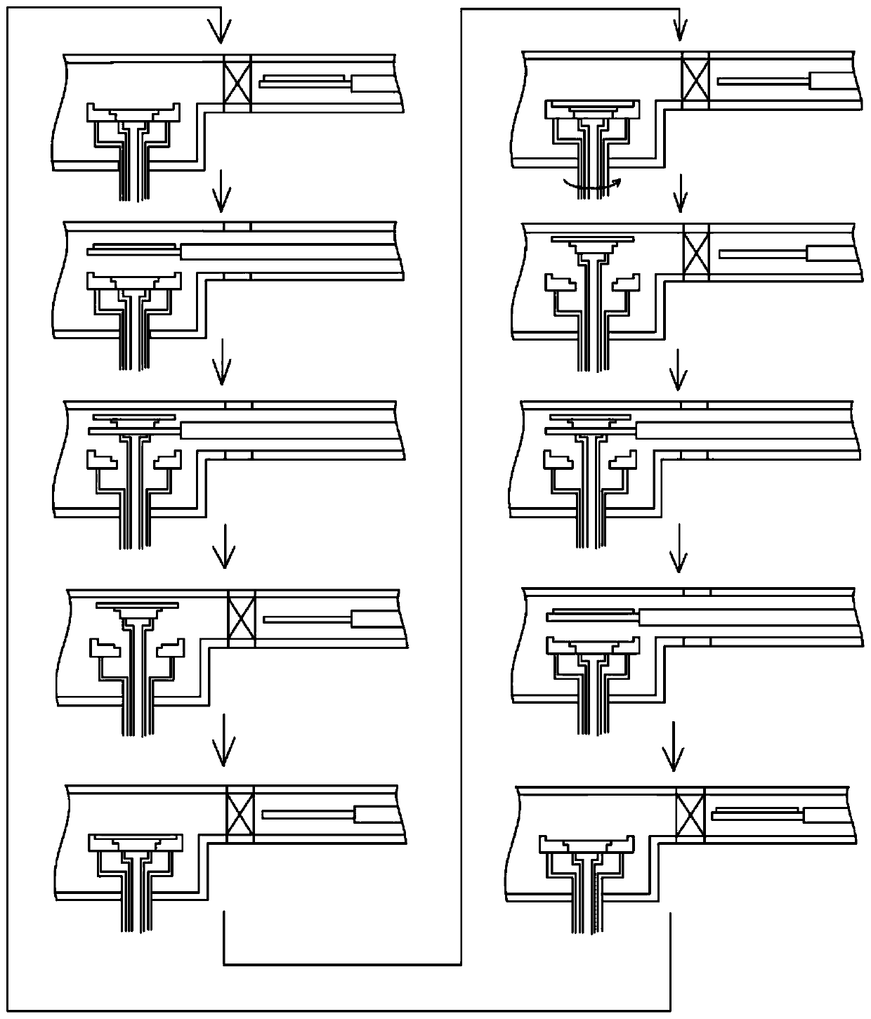
[0033] Below in conjunction with specific embodiment, content of the present invention is described in further detail:

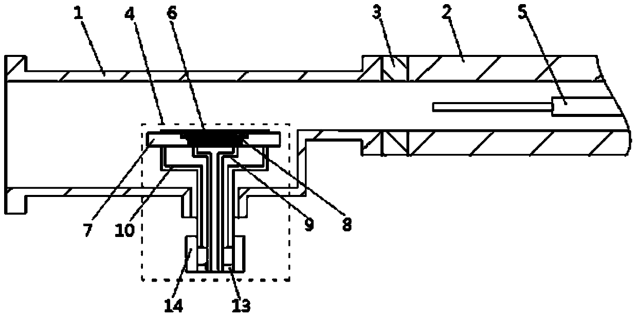
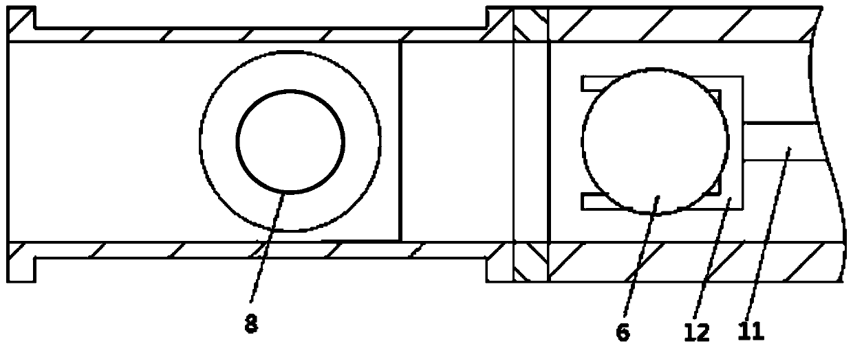
[0034] figure 1 Shown is a cross-sectional view of the front view of the entire structure of the wafer handling device for the reaction chamber. A wafer transmission device for a reaction chamber, comprising: a reaction chamber 1 , a transfer chamber 2 , a gate valve 3 , a wafer support part 4 , a mechanical transfer part 5 and a wafer 6 . Both the reaction chamber 1 and the transfer chamber 2 have a square cavity structure, and they are connected by a gate valve 3 .

[0035] The wafer supporting part 4 includes: an outer ring base 7 , an inner ring base 8 , an inner ring support frame 9 and an outer ring support frame 10 . The inner ring base 8 includes a disc main body, a cylindrical boss is provided on the lower end of the disc, and the overall cross-section is T-shaped. The outer ring base 7 is circular, the inner ring of the outer ring base 7 is step...


PUM


Abstract

The invention relates to the technical field of semiconductor manufacturing equipment, in particular to a wafer transmission device and method for a reaction chamber of the epitaxial growth equipment.The device comprises the reaction chamber and a carrying chamber which are both hollow square cavity structures, the reaction chamber and the carrying chamber are communicated through a gate valve, awafer supporting component is arranged in the reaction chamber, and a mechanical conveying component is arranged in the carrying chamber. The wafer supporting part comprises an inner ring base and anouter ring base, the main body of the inner ring base is a disc, a concentric boss is arranged on the lower end face of the disc, and the overall longitudinal cross section of the inner ring base isT-shaped. The outer ring base is in a circular ring shape, the inner ring of the outer ring base is stepped, the step size of the inner ring is matched with the outer edge size of the inner ring base,and the inner ring base is embedded in the outer ring base. The invention further provides the wafer transmission method for the reaction chamber. The wafer conveying device is easy to operate, is better in conveying stability and lower in wafer falling rate, and can satisfies the conveying requirements of the wafers of different sizes.

Description

technical field [0001] The invention relates to the technical field of semiconductor manufacturing equipment, in particular to a wafer transmission device and a transmission method for a reaction chamber of epitaxial growth equipment. Background technique [0002] The epitaxial growth device mainly picks up the wafer from the magazine through the wafer pick-up mechanism, transports the wafer to the reaction chamber, and places it on a rotatable base. The reaction gas is introduced onto the wafer in a direction parallel to the wafer, and the surface of the wafer Perform epitaxial growth. [0003] The pursuit of larger-diameter epitaxial processing capabilities and higher-quality epitaxial growth effects has become the mainstream of the development of epitaxial wafer production in the world. The current pick-up device using Bernoulli rods is only suitable for small-diameter wafers and cannot meet the needs of wafers of 12 inches and above. [0004] In order to avoid damage t...

Claims


Application Information

Patent Timeline
Patent Type & Authority Applications(China)
IPC IPC(8): H01L21/677H01L21/687H01L21/67
CPCH01L21/67196H01L21/67742H01L21/68785
Inventor 沈文杰朱亮董医芳祝广辉汤承伟俞城麻鹏达周航章杰峰
Owner ZHEJIANG QIUSHI SEMICON EQUIP CO LTD
Why Eureka
Try Eureka