Method and device for determining total dose effect defect model

A technology of total dose effect and defect model, which is applied in the field of microelectronics, can solve the problem that the degradation law of total dose effect of devices cannot be fully characterized, and achieve high-accuracy results

Active Publication Date: 2020-04-07
XIDIAN UNIV
View PDF3 Cites 7 Cited by
  • Summary
  • Abstract
  • Description
  • Claims
  • Application Information

AI Technical Summary

Problems solved by technology

[0005] The present invention provides a method and device for determining the total dose effect defect model to s...

Method used


Image

  • Method and device for determining total dose effect defect model
  • Method and device for determining total dose effect defect model
  • Method and device for determining total dose effect defect model

Examples


Embodiment Construction

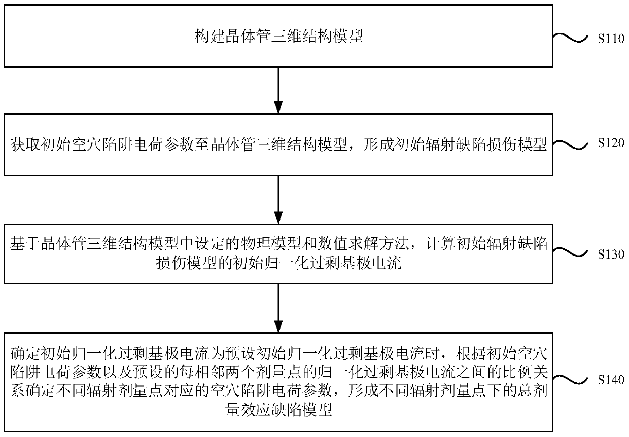
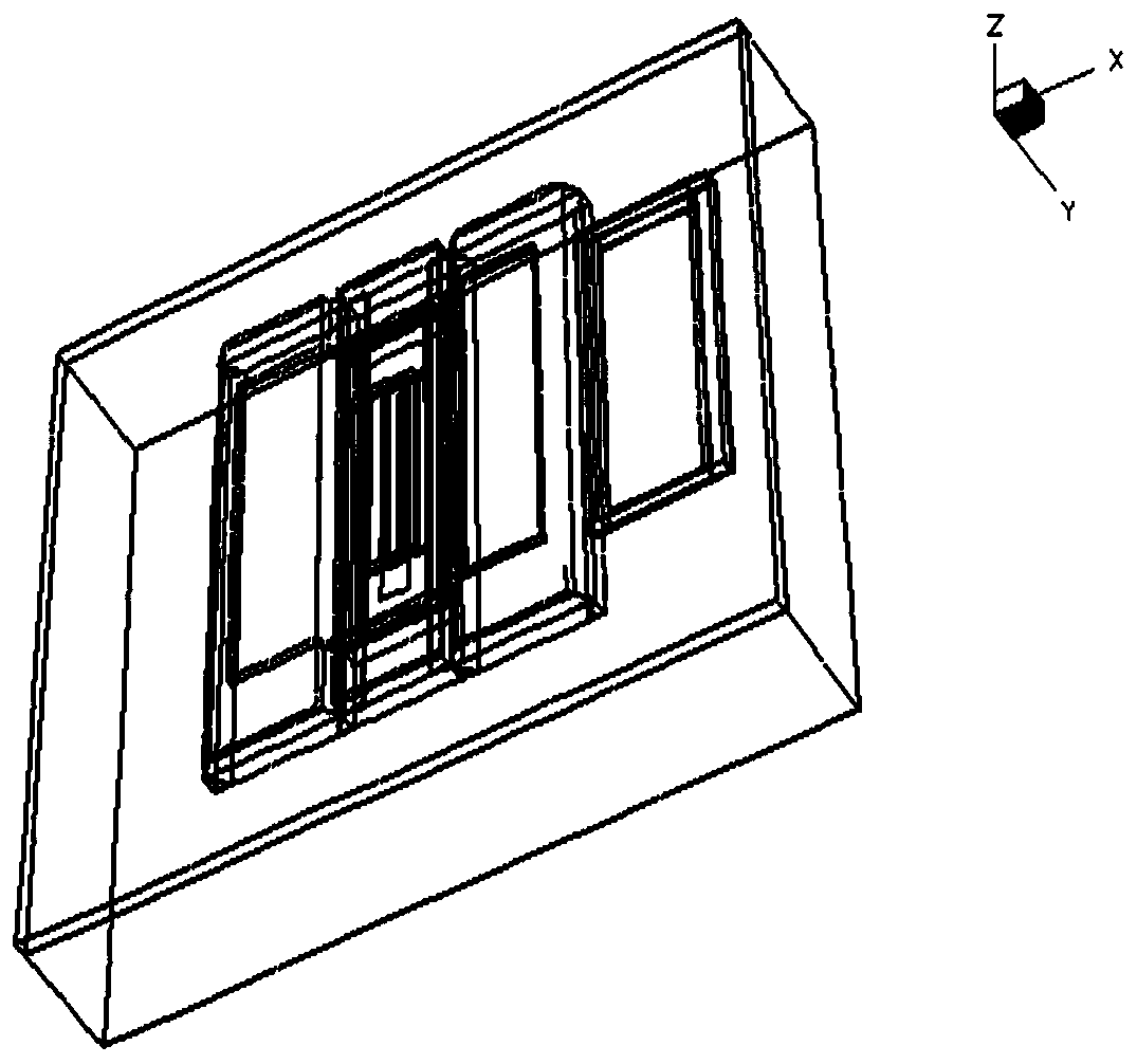
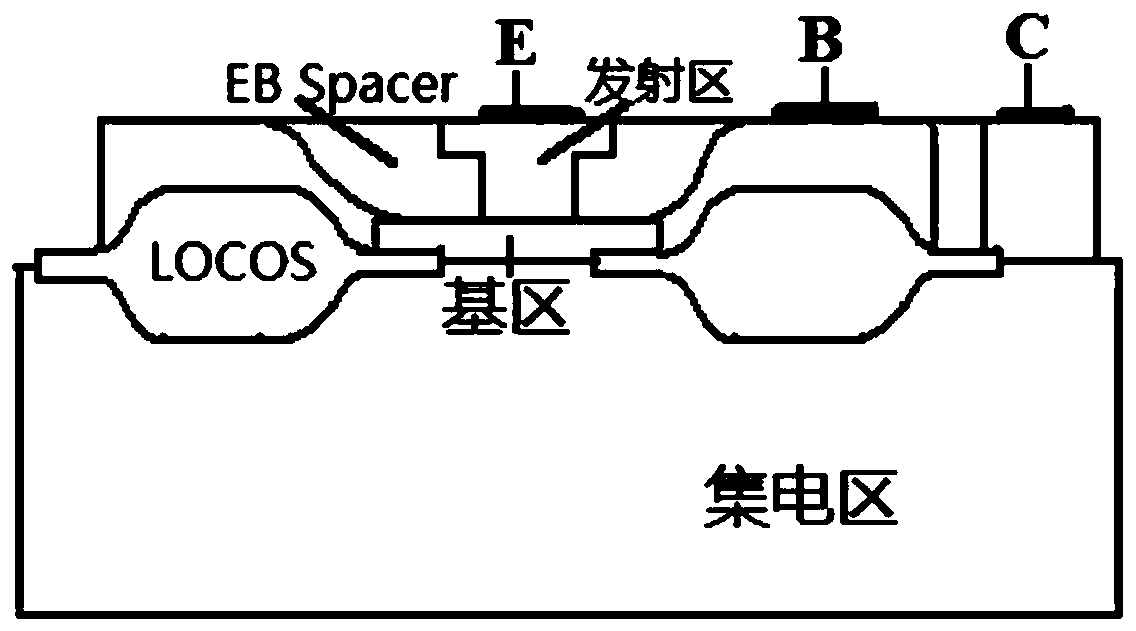
[0063] The present invention will be further described in detail below in conjunction with the accompanying drawings and embodiments. It should be understood that the specific embodiments described here are only used to explain the present invention, but not to limit the present invention. In addition, it should be noted that, for the convenience of description, only some structures related to the present invention are shown in the drawings but not all structures.

[0064] Before describing the technical solutions of the embodiments of the present invention in detail, a brief description will be given of the preset initial normalized excess base current and the preset final normalized excess base current in this embodiment.

[0065] Conduct experiments on the transistor to be tested, set the bias voltage of the transistor to be tested; perform n times on the transistor to be tested with the bias voltage set 60 Co gamma ray irradiation; wherein, the i-th time is performed on t...


PUM


Abstract

The embodiment of the invention discloses a method and device for determining a total dose effect defect model. The method for determining the total dose effect defect model comprises the following steps: constructing a transistor three-dimensional structure model; obtaining an initial hole trapped charge parameter to the transistor three-dimensional structure model to form an initial radiation defect damage model; calculating an initial normalized excess base current of the initial radiation defect damage model based on a physical model and a numerical solution method set in the transistor three-dimensional structure model; determining that the initial normalized excess base current is a preset initial normalized excess base current; and determining hole trap charge parameters corresponding to different radiation dose points according to the initial hole trap charge parameters and a preset proportional relation between normalized excess base currents of every two adjacent radiation dose points, and forming a total dose effect defect model under the different radiation dose points.

Description

technical field [0001] Embodiments of the present invention relate to the field of microelectronic technology, and in particular to a method and device for determining a total dose-effect defect model. Background technique [0002] As an important discrete semiconductor device, bipolar transistor is the core device of bipolar digital and analog integrated circuits, and is widely used in electronic systems of spacecraft. However, microelectronic devices and circuits working in the space environment will inevitably be affected by ionizing radiation from various cosmic rays and high-energy particles, causing performance degradation and bringing major hidden dangers to the reliability of spacecraft electronic systems. Especially when it is applied to the exterior of the satellite shell, the particle radiation suffered in a short period of time increases sharply, and the total dose effect of ionizing radiation becomes a non-negligible damage factor. However, the silicon / silicon ...

Claims


Application Information

Patent Timeline
IPC IPC(8): G06F30/20G06T17/00
CPCG06T17/00Y02E60/00
Inventor 张晋新郭红霞任迪远付军王玉东潘霄宇王辉冯娟
Owner XIDIAN UNIV
Why Eureka
Try Eureka