Supercharge Your Innovation With Domain-Expert AI Agents!

Current monitoring device and method for CMOS device

A current monitoring and device technology, applied in measuring devices, measuring current/voltage, instruments, etc., can solve problems such as affecting the life of CMOS devices, burning CMOS devices, damaging application systems, etc., achieving low cost, reducing floor space, high precision effect

Inactive Publication Date: 2020-04-10
上海微阱电子科技有限公司
View PDF8 Cites 0 Cited by
  • Summary
  • Abstract
  • Description
  • Claims
  • Application Information

AI Technical Summary

Problems solved by technology

[0002] Each CMOS device in the integrated circuit usually uses the control module to control the power supply module to supply power to the CMOS device during the working process. However, during the working process of the CMOS device, there is no effective device or method to monitor its working status, and it usually needs to wait until the CMOS device outputs After the results are obtained, the work status can be judged according to the results
[0003] Due to the large number of applications of CMOS devices and the uncertainty of environmental parameters, their working status will also be affected. If the current of the CMOS device changes greatly due to changes in the external environment and its own configuration during its work , if the working current in the CMOS device increases sharply, the power consumption of the CMOS device will increase and seriously affect the life of the CMOS device, and it will burn the CMOS device or even damage the entire application system. Therefore, the DC parameters of the CMOS device, especially the current parameters Monitoring is becoming more and more important

Method used


Image

  • Current monitoring device and method for CMOS device
  • Current monitoring device and method for CMOS device
  • Current monitoring device and method for CMOS device

Examples


Embodiment 1

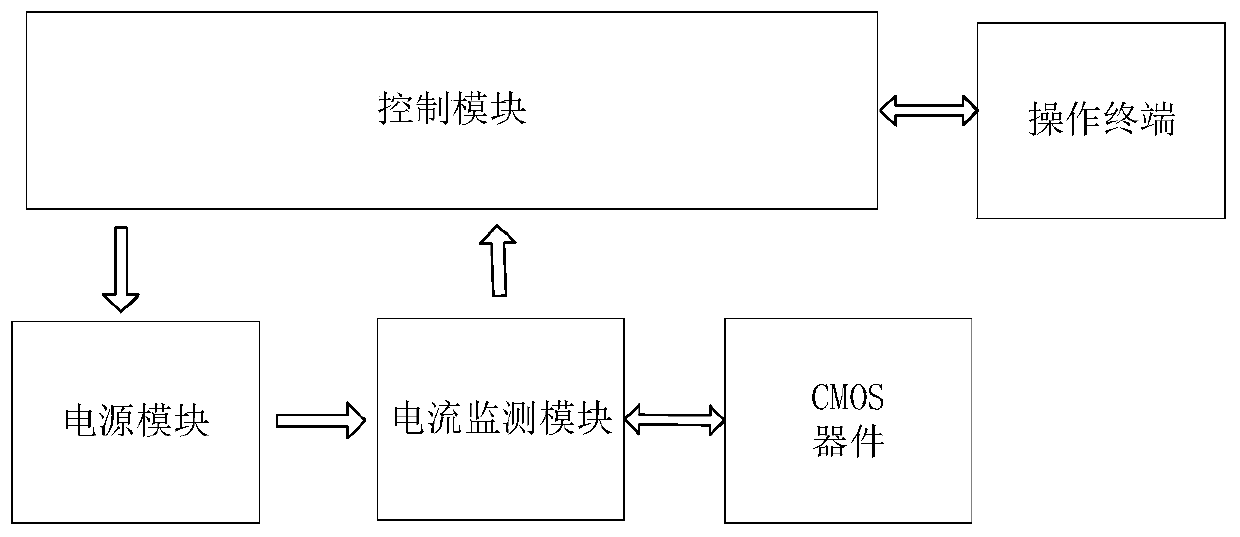
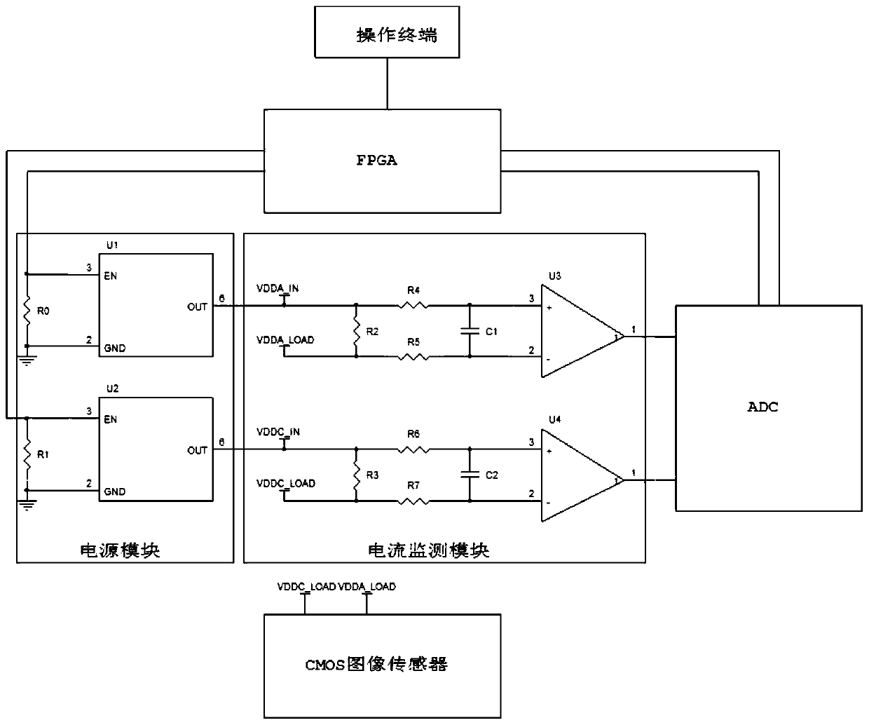
[0043] Please refer to the attached image 3 , the CMOS device is a CMOS image sensor, the control module is an FPGA, and the FPGA includes an ADC; and the output terminal of the current monitoring module is connected to the ADC, and the analog signal output by the current monitoring module is converted into a digital signal by the ADC. In this embodiment, the power supply module includes an analog power supply unit and a digital power supply unit. The analog power supply unit includes a power chip U1 and a drop resistor R0. The two input terminals of the power chip U1 are respectively connected to both ends of the drop resistor R0. The drop resistor R0 Both ends of the power chip U1 are grounded and connected to the control module, so that one end of the power chip U1 receives the enable signal of the FPGA, and the other end is grounded. The digital power supply unit includes a power chip U2 and a drop-down resistor R1. The two input ends of the power chip U2 are respectively...

Embodiment 2

[0054] Please refer to the attached Figure 4 , the CMOS device is a CMOS memory device, the control module is a DSP, and the DSP includes an ADC, and the output terminal of the current monitoring module is connected to the ADC, and the analog signal output by the current monitoring module is converted into a digital signal through the ADC. In this embodiment, the power supply module includes four power supply units. The first power supply unit includes a power supply chip U8 and a drop-down resistor R8. The two input terminals of the power supply chip U8 are respectively connected to both ends of the drop-down resistor R8. The ends are respectively grounded and connected to the control module, so that one end of the power chip U8 receives the enable signal of the DSP, and the other end is grounded.

[0055] The second power supply unit includes a power chip U9 and a voltage-dropping resistor R9. The two input ends of the power chip U9 are respectively connected to the two end...


PUM


Abstract

A current monitoring device of a CMOS device comprises the CMOS device, a current monitoring module, a power supply module and a control module, wherein the control module is connected with the powersupply module and the current monitoring module at the same time, and the power supply module is connected with the CMOS device through the current monitoring module; the power supply module suppliespower to the CMOS device through the current monitoring module; the current monitoring module monitors the supply current in the working state of the CMOS device in real time and sends the monitoringresult to the control module; and when the monitoring result is abnormal, the control module controls the power supply module to stop supplying power. According to the current monitoring device and the method for the CMOS device, the current of the CMOS device can be conveniently and accurately monitored in real time, and a reference basis is provided for stable work of the CMOS device and even chip design and process improvement.

Description

technical field [0001] The invention relates to the field of integrated circuit testing, in particular to a current monitoring device and method for a CMOS device. Background technique [0002] Each CMOS device in the integrated circuit usually uses the control module to control the power supply module to supply power to the CMOS device during the working process. However, during the working process of the CMOS device, there is no effective device or method to monitor its working status, and it usually needs to wait until the CMOS device outputs After the results are obtained, the work status can be judged according to the results. [0003] Due to the large number of applications of CMOS devices and the uncertainty of environmental parameters, their working status will also be affected. If the current of the CMOS device changes greatly due to changes in the external environment and its own configuration during its work , if the working current in the CMOS device increases s...

Claims


Application Information

Patent Timeline
Patent Type & Authority Applications(China)
IPC IPC(8): G01R19/00G01R19/25
CPCG01R19/00G01R19/25
Inventor 姚清志卢意飞
Owner 上海微阱电子科技有限公司
Features
  • R&D
  • Intellectual Property
  • Life Sciences
  • Materials
  • Tech Scout
  • Unparalleled Data Quality
  • Higher Quality Content
  • 60% Fewer Hallucinations
Learn More