Impedance balance degree analysis method of on-chip power combiner

A technology of power combiner and impedance balance, which is applied in the direction of instruments, special data processing applications, electrical digital data processing, etc. It can solve problems such as time-consuming, inability to analyze balance mismatch, etc., and achieve the effect of less hardware and software resources

Active Publication Date: 2020-04-10
SOUTHEAST UNIV +2
View PDF4 Cites 0 Cited by
  • Summary
  • Abstract
  • Description
  • Claims
  • Application Information

AI Technical Summary

Problems solved by technology

This method needs to consume a lot of computer hardware and software resources, and it will also take a lot of time, and for the designer, it is impossible to analyze the cause of the balance mismatch by using this method

Method used


Image

  • Impedance balance degree analysis method of on-chip power combiner
  • Impedance balance degree analysis method of on-chip power combiner
  • Impedance balance degree analysis method of on-chip power combiner

Examples


Embodiment Construction

[0029] The present invention will be further described below in conjunction with the accompanying drawings and specific embodiments.

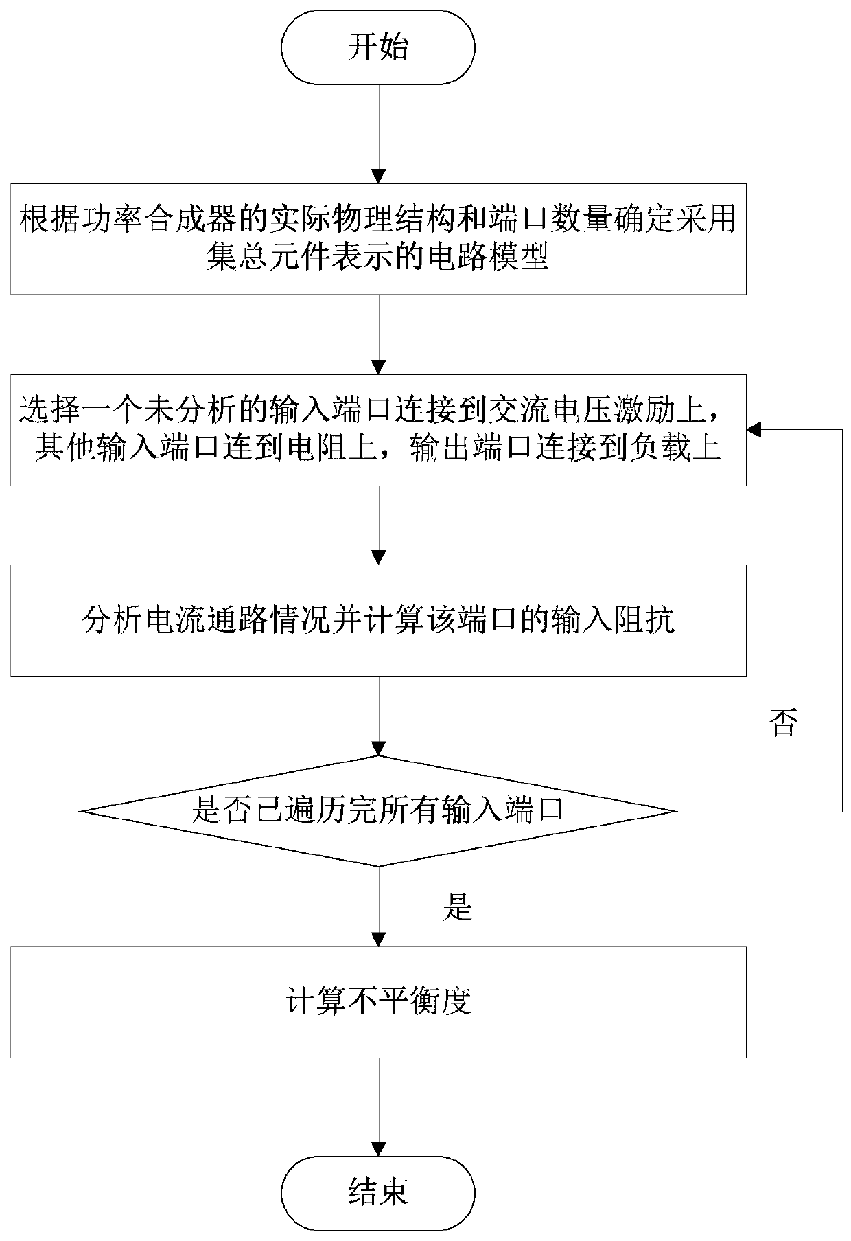
[0030] like figure 1 As shown, an impedance balance analysis method of an on-chip power combiner disclosed in an embodiment of the present invention, the steps include:

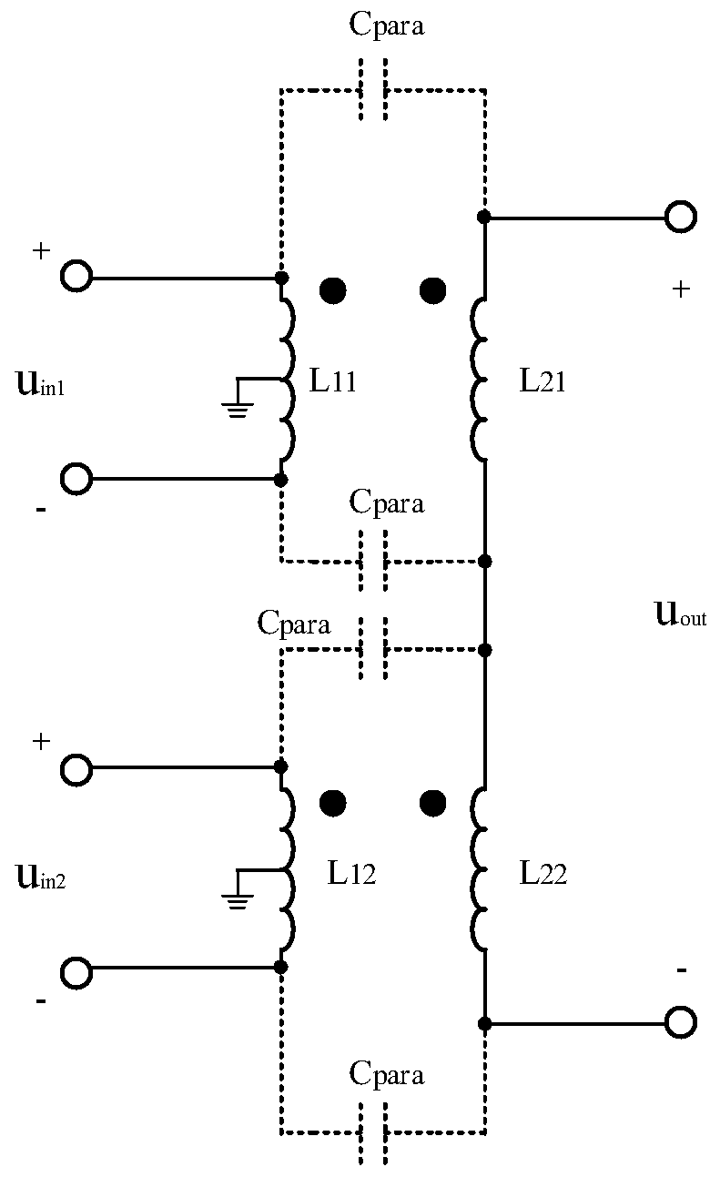
[0031] (1) According to the actual physical structure and number of ports of the power combiner, determine the circuit model represented by lumped elements, the model includes interlayer parasitic capacitance and transformer, and has N (N≥2) input ports and one output port , and the electromagnetic coupling between the coils is represented by a controlled current source connected across the output coil;

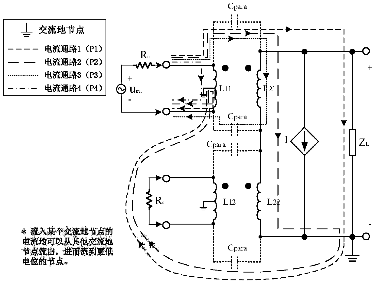
[0032] (2) Select one of the N input ports and connect it to an internal resistance R s The AC voltage excitation; connect the other N-1 input ports to N-1 resistances R s on the resistor; connect the output port to the load Z L superior;

[0033] (3) Analyze the path of...


PUM


Abstract

The invention discloses an impedance balance degree analysis method of an on-chip power combiner. The method comprises the following steps: firstly, determining a circuit model represented by lumped elements according to an actual physical structure and the number of ports of the power combiner; then, an input port is connected to an alternating voltage exciter; other input ports are connected toa resistor, an output port is connected to a load, a current path is analyzed, the input impedance of the corresponding input port is calculated, an alternating current ground node is regarded as an intermediate node of the current path in the analysis process, the path of the current path is determined by searching the minimum branch current, and the impedance on the path is calculated; and finally, calculating the balance degree between the input ports according to the input impedance of each port and the expression of the balance degree. Compared with a traditional method that a large number of computers and time resources are needed for simulation analysis, when the method is used for analyzing the on-chip power combiner, the process is simpler and more convenient, consumed time is shorter, and the source of balance degree mismatch can be found.

Description

technical field [0001] The invention relates to an analysis method of a passive device, in particular to an analysis method of an impedance balance degree of an on-chip power combiner. Background technique [0002] Impedance balance is a qualitative measure of the difference in input impedance in most circuit analysis scenarios, but there are also a few that have been published in conferences and journals in the field of integrated circuits. The difference between the input impedance of any two ports divided by the sum of the input impedance To quantitatively describe and compare the definition of balance. The input impedance refers to a complex impedance including a real part and an imaginary part, which is defined as the voltage on the complex plane divided by the current on the complex plane. [0003] However, for the calculation and evaluation of the degree of balance, the current mainstream methods are still in the simulation analysis using various software. The core o...

Claims


Application Information

Patent Timeline
IPC IPC(8): G06F30/367
Inventor 袁灿然张有明唐旭升魏震楠黄风义姜楠
Owner SOUTHEAST UNIV
Why Eureka
Try Eureka