
Dry etching method

A dry etching, to-be-etched technology, applied in electrical components, semiconductor/solid-state device manufacturing, circuits, etc., can solve the problem of inconsistent openings in the central and edge regions of the wafer and poor uniformity of the wafer surface etching morphology , load high temperature alarm and other problems, to avoid high temperature alarm situation, uniform appearance, and ensure the effect of stable progress

Active Publication Date: 2020-04-17
苏州科阳半导体有限公司
View PDF8 Cites 1 Cited by
  • Summary
  • Abstract
  • Description
  • Claims
  • Application Information

AI Technical Summary

Problems solved by technology

[0004]However, when the thickness of the silicon is larger, the uniformity of the etching morphology on the wafer surface is poorer, and the opening sizes of the central area and the edge area of ​​the wafer are inconsistent. Moreover, mass production cannot be stabilized by one-step etching, and the machine will generate a load high temperature alarm

Method used


Image

  • Dry etching method
  • Dry etching method
  • Dry etching method

Examples


Embodiment Construction

[0036] The present invention will be further described in detail below in conjunction with the accompanying drawings and embodiments. It should be understood that the specific embodiments described here are only used to explain the present invention, but not to limit the present invention. In addition, it should be noted that, for the convenience of description, only some structures related to the present invention are shown in the drawings but not all structures.

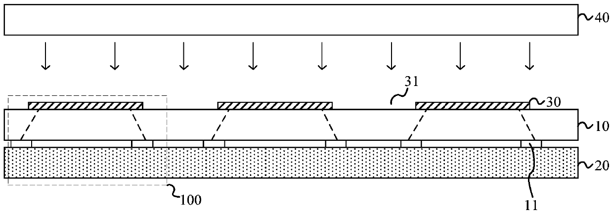
[0037] figure 1 It is a schematic diagram of the working principle of the dry etching process. Before introducing this scheme, first combine figure 1 The working process of dry etching in wafer packaging process is introduced.

[0038] like figure 1 As shown, the working surface of the wafer 10 to be etched is provided with metal electrodes 11 corresponding to each chip 100 , and the working surface of the wafer 10 to be etched further includes a glass cover 20 protecting the working surface of the wafer. In th...


PUM


Abstract

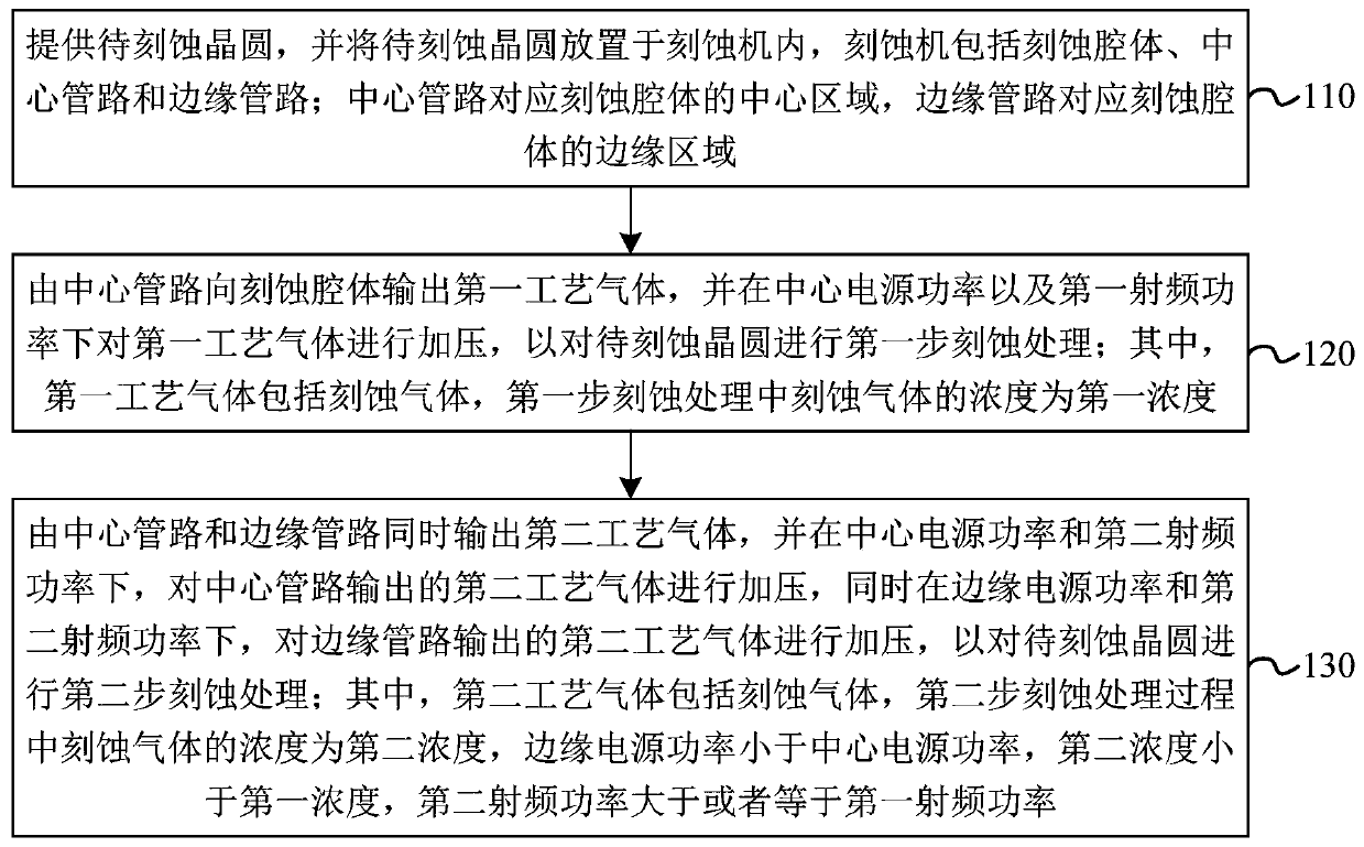
The embodiment of the invention discloses a dry etching method. The dry etching method comprises the following steps: providing a wafer to be etched and placing the wafer in an etching machine; outputting process gas to the etching cavity from a central pipeline, and pressurizing the process gas under the power of the central power supply and the first radio frequency power so as to carry out first-step etching treatment; simultaneously outputting process gas by the central pipeline and the edge pipeline, pressurizing the process gas output by the central pipeline under the central power supply power and the second radio frequency power, and pressurizing the process gas output by the edge pipeline under the edge power supply power and the second radio frequency power so as to carry out second-step etching treatment, wherein the process gas comprises etching gas, the concentration of the etching gas in the second-step etching treatment is smaller than that of the etching gas in the first-step etching treatment, the edge power supply power is smaller than the central power supply power, and the second radio frequency power is larger than or equal to the first radio frequency power. According to the method, the morphology of each region of the etched wafer is relatively uniform.

Description

technical field [0001] Embodiments of the present invention relate to semiconductor processing technologies, and in particular to a dry etching method. Background technique [0002] The dry etching process is often used in the field of wafer manufacturing or wafer advanced packaging. The dry etching gas reacts with the silicon on the back of the wafer to etch groove or hole structures. [0003] However, the existing dry etching process is usually formed in one step, and the gas in the central pipeline is used to perform rapid etching on the wafer to obtain the final etched shape. [0004] However, when the thickness of the silicon is larger, the uniformity of the etching morphology on the wafer surface is poorer, and the opening sizes in the center area and the edge area of ​​the wafer are inconsistent. Moreover, mass production cannot be stabilized by one-step etching. In case of load high temperature alarm. Contents of the invention [0005] An embodiment of the presen...

Claims


Application Information

Patent Timeline
IPC IPC(8): H01L21/3065H01L21/67
CPCH01L21/3065H01L21/67253
Inventor 李树宏李三三刘一川汤伟杰
Owner 苏州科阳半导体有限公司
Learn More