Manufacturing method of 5G signal shielding PCB module with latches

A technology of signal shielding and production methods, which is applied in the fields of printed circuit manufacturing, electrical components, printed circuits, etc., can solve problems such as difficult to guarantee the quality of mass production, and achieve the effects of fast delivery, cost reduction, and production efficiency improvement

Active Publication Date: 2020-04-17
HUIZHOU KING BROTHER CIRCUIT TECH +2
View PDF6 Cites 5 Cited by
  • Summary
  • Abstract
  • Description
  • Claims
  • Application Information

AI Technical Summary

Problems solved by technology

In order to achieve the requirement that the tolerance of the finished product is ≤0.05mm, it is difficult to meet the current conventional process, especially the quality of mass production is difficult to guarantee

Method used


Image

  • Manufacturing method of 5G signal shielding PCB module with latches
  • Manufacturing method of 5G signal shielding PCB module with latches
  • Manufacturing method of 5G signal shielding PCB module with latches

Examples


Embodiment

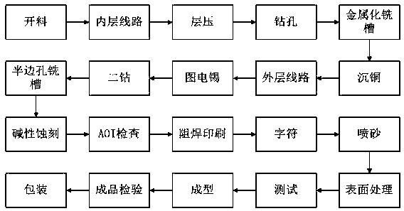
[0034] A method for manufacturing a 5G signal shielding PCB module with locking teeth, comprising the following steps:

[0035] S1. Main process: In the main process, when the AOI inspection is performed on the line after the outer layer is etched, in addition to the routine inspection, the inspection of copper particles and pinholes is added to ensure that the product has no pinholes and voids, so that the product has a good signal shielding function ;

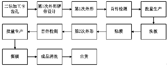
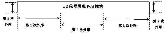
[0036] S2. Forming processing sub-process: Half hole milling and metallization milling must be done according to the expansion and contraction of the drilling file to ensure the shape and accuracy of the slot; Necessary conditions for the final processing accuracy of products without internal positioning to be qualified;

[0037] S3. Clamp tooth size processing: the diameter of the half hole at the root of both sides of the clamp tooth is 0.1-1mm, use the second dimension to test the expansion and contraction of the product ...


PUM


Abstract

The invention belongs to the technical field of PCB processing, and provides a manufacturing method of a 5G signal shielding PCB module with latches. The method comprises the following steps of: S1, amain process; s2, a forming processing sub-process; S3, latch size processing; S4, forming size processing; and S5, size and appearance quality detection. The 5G signal shielding effect is guaranteed, meanwhile, the latch size is controlled within + / -0.05mm, no gap after the latches and clamping grooves are highly matched and welded is guaranteed, and the 100% shielding effect on signals is achieved.

Description

technical field [0001] The invention belongs to the technical field of PCB processing, and in particular relates to a method for manufacturing a 5G signal shielding PCB module with locking teeth. Background technique [0002] In the 5G network, the priority layout is the network base station, and the core product related to PCB is the processing of MIMO array antenna products, and the number and units have independent transceiver capabilities. In order to prevent the signals from interfering with each other, it is necessary to make a PCB product between each unit and connect it to the main PCB to isolate the signal. This type of product requires the PCB material to be rigid and flexible, and the whole board has no positioning holes, and the surrounding The dimensional accuracy of the teeth is less than or equal to 0.05mm, super long (aspect ratio > 20:1), ultra-thin (thickness < 0.5mm) and other characteristics. However, it is very difficult to achieve this requirem...

Claims


Application Information

Patent Timeline
IPC IPC(8): H05K3/00
CPCH05K3/0044H05K3/0047
Inventor 聂兴培武守坤吴世亮李享
Owner HUIZHOU KING BROTHER CIRCUIT TECH
Why Eureka
Try Eureka