PCB online semiconductor device testing system

A PCB board and testing system technology, applied in the field of PCB board online semiconductor device testing system, can solve the problems of lower assembly efficiency, lower work efficiency, lower detection efficiency, etc., and achieve simple and convenient overall structure, simplified detection process, and improved detection efficiency effect

Active Publication Date: 2020-04-21
深圳市瑞福自动化设备有限公司
View PDF9 Cites 4 Cited by
  • Summary
  • Abstract
  • Description
  • Claims
  • Application Information

AI Technical Summary

Problems solved by technology

[0003] At present, the equipment for automatic detection of PVB boards is mainly a functional tester, which ensures that the performance of the PCB board is normal through systematic detection. However, during the detection process of the PCB board, the clamping action of the entire PCB board is not There is no suitable fixture to match it, and each fixture is suitable for its corresponding model, so in the process of testing different types of PCB boards, the assembly efficiency is reduced, and the fixtures used cannot be compatible with most fixtures Therefore, the inspection efficiency is reduced, the entire inspection process is cumbersome and complicated, and at the same time, the work efficiency is significantly reduced, so it cannot meet the work requirements.

Method used


Image

  • PCB online semiconductor device testing system
  • PCB online semiconductor device testing system
  • PCB online semiconductor device testing system

Examples


Embodiment Construction

[0024] The following will clearly and completely describe the technical solutions in the embodiments of the present invention with reference to the accompanying drawings in the embodiments of the present invention. Obviously, the described embodiments are only some, not all, embodiments of the present invention. Based on the embodiments of the present invention, all other embodiments obtained by persons of ordinary skill in the art without making creative efforts belong to the protection scope of the present invention.

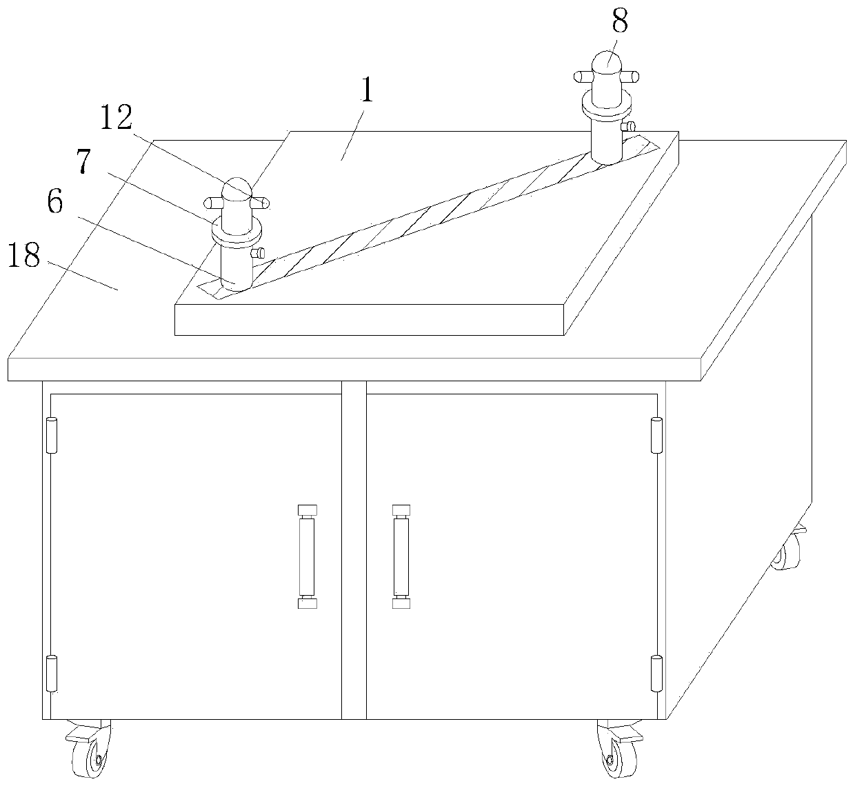
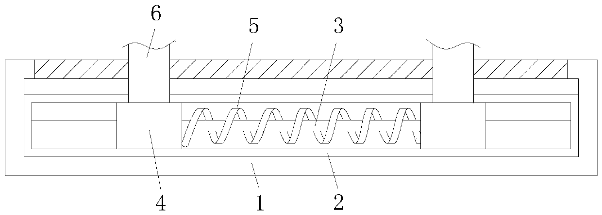
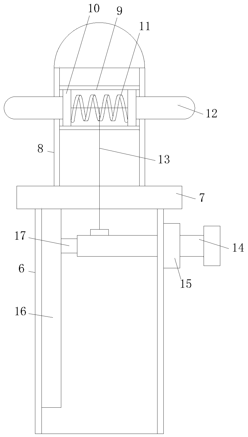
[0025] see Figure 1-4 , the present invention provides a technical solution: a PCB board online semiconductor device testing system, including a placement table 1, a sliding rod 3, a sliding sleeve 4, a telescopic spring 5, a movable rod 6, a limit plate 7, a plug post 8, Slide rail 9, slider 10, extrusion spring 11, limit post 12, rope 13, adjustment screw 14, lock nut 15, guide rail 16, movable block 17, needle bed 18 and test system 19, and the inner wall ...


PUM


Abstract

The invention relates to the technical field of PCBs and especially relates to a PCB online semiconductor device testing system. The system comprises a placement table, a sliding rod, sliding sleeves,a telescopic spring, a movable rod, a limiting plate, an insertion column, a sliding rail, a sliding block, an extrusion spring, a limiting column, a rope, an adjusting screw rod, a locking nut, a guide rail, a movable block, a needle bed and a testing system. A sliding groove is arranged in a bottom of an inner wall of the placement table, middle positions of the two sides of the inner wall of the sliding groove are fixedly connected with two ends of the sliding rod correspondingly, the two sliding sleeves are connected with an outer surface of the sliding rod in a sleeving mode correspondingly, and the sliding sleeves are slidably connected with the sliding rod. In the invention, a purpose that the system is suitable for clamping and positioning PCBs of different models and sizes is achieved; and meanwhile, an overall structure is simple and convenient, automatic change can be performed according to the size, and a mode that clamps need to be replaced according to models in the pastwhen the PCB is detected is replaced so that detection efficiency is improved, a detection procedure is simplified, and a clamping requirement in a PCB detection process is met.

Description

technical field [0001] The invention relates to the technical field of PCB boards, in particular to a PCB board online semiconductor device testing system. Background technique [0002] Circuit boards have become an important part of today's electronic products. With the development of electronic technology and printed circuit board manufacturing technology, modern electronic products are becoming more and more complex, and the density of printed circuit boards is increasing. Testing and repairs are also more difficult. In order to improve the automation degree of inspection and maintenance of printed circuit boards, it is very necessary to design an automatic test system for circuit boards. [0003] At present, the equipment for automatic detection of PVB boards is mainly a functional tester, which ensures that the performance of the PCB board is normal through systematic detection. However, during the detection process of the PCB board, the clamping action of the entire P...

Claims


Application Information

Patent Timeline
Patent Type & Authority Applications(China)
IPC IPC(8): G01R31/28G01R31/26G01R1/04
CPCG01R31/2801G01R31/2818G01R31/2601G01R1/0425
Inventor 肖国梁
Owner 深圳市瑞福自动化设备有限公司
Why Eureka
Try Eureka