Polycrystalline silicon film deposition method

A polycrystalline silicon thin film and deposition method technology, which is applied in the growth of polycrystalline materials, chemical instruments and methods, crystal growth, etc., can solve the problems of limited effect and narrow temperature adjustable range.

Pending Publication Date: 2020-04-21
SHANGHAI HUALI MICROELECTRONICS CORP
View PDF15 Cites 0 Cited by
  • Summary
  • Abstract
  • Description
  • Claims
  • Application Information

AI Technical Summary

Problems solved by technology

However, in the actual production process, the temperature adjustable range is relatively narrow, about 600°C-620°C. If you deviate from this temperature range, you may end up with amorphous silicon i

Method used


Image

  • Polycrystalline silicon film deposition method

Examples


Embodiment Construction

[0022] The specific embodiments of the present invention will be described in more detail below with reference to the schematic diagram. According to the following description, the advantages and features of the present invention will become clearer. It should be noted that the drawings are in a very simplified form and all use imprecise proportions, which are only used to conveniently and clearly assist in explaining the purpose of the embodiments of the present invention.

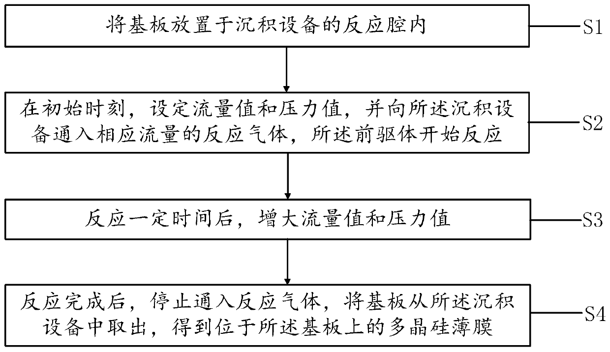
[0023] In order to effectively control the crystal grain size during the formation of the polysilicon film, an embodiment of the present invention provides a method for depositing a polysilicon film. In this embodiment, the polysilicon film is, for example, an undoped polysilicon film. The deposition method of the polysilicon film can be used in low pressure chemical vapor deposition (LPCVD). The LPCVD process is a method commonly used in the production of polysilicon films in integrated circuits. The depos...


PUM


Abstract

The invention provides a polycrystalline silicon film deposition method. The deposition method comprises the following steps: firstly, placing a substrate in the reaction cavity of deposition equipment; then setting a flow value and a pressure value before the reaction is started, and introducing a reaction gas with a corresponding flow into the deposition equipment so that the reaction gas startsto react; after reacting for a certain time, increasing the flow value and the pressure value; and then, after the reaction is finished, stopping introducing the reaction gas, and taking out the substrate from the equipment to obtain the polycrystalline silicon thin film on the substrate. According to the polycrystalline silicon film deposition method, the quantity of crystal grain nucleation canbe controlled by controlling the flow and the pressure of the reaction gas inputted into the reaction cavity at the initial moment of the reaction so that the purpose of controlling the crystal grainsize of the polycrystalline silicon thin film is achieved; and compared with the method of controlling the grain size by controlling the reaction temperature, the method is more flexible, and the range of the adjustable grain size is wider.

Description

Technical field [0001] The invention relates to the field of semiconductor manufacturing, in particular to a deposition method of a polysilicon film. Background technique [0002] Polysilicon films are widely used in semiconductor devices. Polysilicon not only has high reliability and is not easy to fuse, but also has good Si-SiO 2 Interface characteristics, its leakage current is very small when surrounded by insulating materials, and more importantly, the polysilicon manufacturing process is simple, which reduces the process level of the device. Therefore, polysilicon is an ideal material for gates and local interconnections in integrated circuit technology. [0003] Polycrystalline silicon film is composed of multiple crystal grains. There are grain boundaries between different crystal grains. The grain boundaries are the transition regions from one grain to another along a certain crystal direction. Its structure is complex. Atoms are arranged in disorder, usually a few atomic ...

Claims


Application Information

Patent Timeline
IPC IPC(8): H01L21/3205H01L21/285H01L21/768C30B28/14C30B29/06
CPCH01L21/28556H01L21/32055H01L21/76838C30B29/06C30B28/14
Inventor 聂广宇
Owner SHANGHAI HUALI MICROELECTRONICS CORP
Why Eureka
Try Eureka