Control of crystal grain size of polysilicon film and detecting method thereof

A polysilicon thin film, grain size technology, applied in measurement devices, semiconductor/solid-state device testing/measurement, material analysis by optical means, etc., can solve the problem of inability to accurately obtain laser energy density and crystallization rate

Inactive Publication Date: 2004-06-02
AU OPTRONICS CORP
View PDF0 Cites 9 Cited by
  • Summary
  • Abstract
  • Description
  • Claims
  • Application Information

AI Technical Summary

Problems solved by technology

However, the above methods cannot accurately obtain the optimal laser energy density and crystallization ratio, especially when the polysilicon film is in super lateral growth (SLG)

Method used


Image

  • Control of crystal grain size of polysilicon film and detecting method thereof
  • Control of crystal grain size of polysilicon film and detecting method thereof
  • Control of crystal grain size of polysilicon film and detecting method thereof

Examples


Embodiment Construction

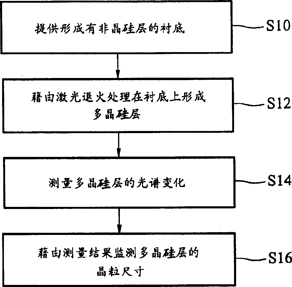
[0023] figure 1 is a flow chart illustrating a polysilicon thin film detection method according to an embodiment of the present invention. First, step S10 is performed to provide a substrate, such as a transparent glass substrate, on which an amorphous silicon (α-Si) layer is formed. In this embodiment, this substrate is used to fabricate a thin film transistor liquid crystal display (TFT-LCD). The amorphous silicon layer on the substrate is used for subsequent fabrication of the channel layer of the thin film transistor. The amorphous silicon layer can be formed by chemical vapor deposition (CVD) or other methods, and its thickness is in the range of about 300 to 1000 angstroms (Å).

[0024] Next, step S12 is performed to anneal the amorphous silicon layer with a laser with a predetermined energy density, such as excimer laser annealing (ELA), to convert the amorphous silicon layer into a polysilicon (p-Si) layer . In this embodiment, the predetermined energy density of t...


PUM


Abstract

The invention discloses a polycrystalline silicon thin film crystal particle size control and detecting method comprising, providing a first substrate covered by a first non-crystalline silicon layer, implementing annealing treatment to the first non-crystalline silicon layer using laser rays of dissimilar energy density to form a plurality of first polycrystalline silicon areas, measuring the light spectrum change of each first polycrystalline silicon area with a finite photon energy range, providing a second substrate covered by a second non-crystalline silicon layer, implementing annealing treatment to the first non-crystalline silicon layer using the above laser energy density to obtain largest polycrystalline silicon crystal particle dimension, and detecting its crystal particle dimension using an elliptical instrument.

Description

technical field [0001] The present invention relates to a method for testing semiconductor thin films, in particular to a method for using an ellipsometer to detect whether the grain size of polysilicon thin films meets specifications, so as to improve device characteristics and yield by controlling laser energy density for crystallization. Background technique [0002] The current thin film transistor-liquid crystal display (TFT-LCD) technology is divided into two types, one is a traditional amorphous silicon thin film transistor, and the other is a polysilicon thin film transistor. The electron movement speed of the polysilicon thin film transistor is between 10 times and 100 times that of the amorphous silicon thin film transistor. Therefore, the TFT-LCD industry has begun research and development, using polysilicon thin film transistors as pixel switching elements and driving circuits around the LCD. [0003] The above-mentioned polysilicon thin film transistors are gen...

Claims


Application Information

Patent Timeline
Patent Type & Authority Applications(China)
IPC IPC(8): G01N21/00H01L21/66
Inventor 林昆志廖龙盛徐振洲
Owner AU OPTRONICS CORP
Why Eureka
Try Eureka