Fan-out type packaging method and fan-out type packaging structure of embedded chip

A packaging method and packaging structure technology, which are applied to semiconductor/solid-state device components, semiconductor devices, electrical components, etc., can solve the problems of reducing the size of the packaging structure of the chip, many process steps, and complex processes, and achieve less interference. , less process steps, the effect of meeting development needs

Inactive Publication Date: 2020-04-21
HUATIAN TECH KUNSHAN ELECTRONICS
View PDF6 Cites 2 Cited by
  • Summary
  • Abstract
  • Description
  • Claims
  • Application Information

AI Technical Summary

Problems solved by technology

[0005] Stacking and packaging at least two layers of chips can greatly reduce the size of the chip packaging structure. For example, the Chinese invention patent with the publication number CN109801883A discloses a fan-out stack packaging method and structure, and the Chinese invention patent with the publication number CN105529276A discloses Low-cost multi-layer stacked fan-out packaging structure and its preparation method. However, these existing stacked packaging methods have many process steps, complicated procedures and relatively high costs

Method used


Image

  • Fan-out type packaging method and fan-out type packaging structure of embedded chip
  • Fan-out type packaging method and fan-out type packaging structure of embedded chip
  • Fan-out type packaging method and fan-out type packaging structure of embedded chip

Examples


specific Embodiment 1

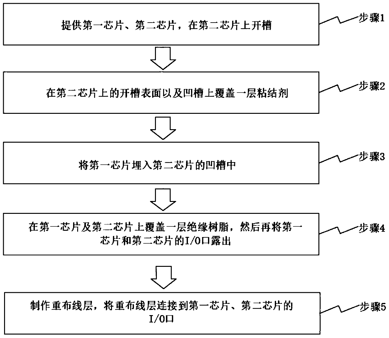
[0058] A fan-out packaging method for embedded chips of the present invention specifically includes the following steps:

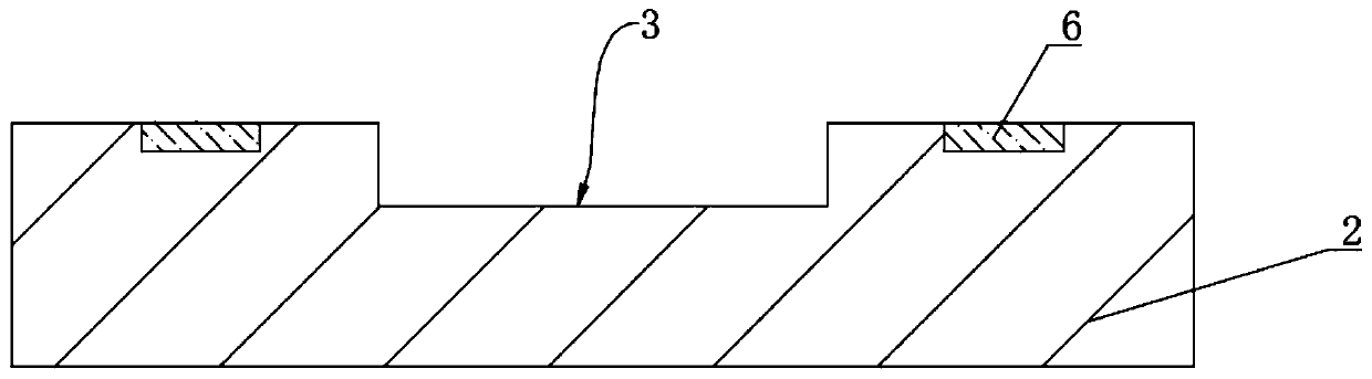
[0059] See figure 2 , step 1: provide the first chip 1 and the second chip 2, first form an opening on the second chip 2 through a photolithography process, and then etch a groove 3 at the position of the opening through an etching process, avoiding the second chip when slotting Functional area on chip 2;

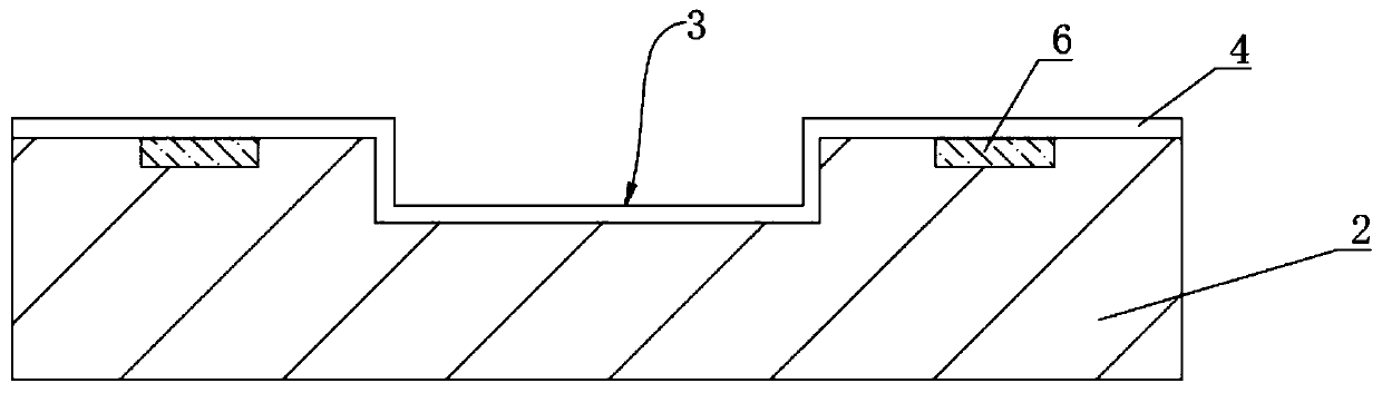
[0060] See image 3 , step 2: cover the grooved surface and the groove on the second chip 2 with a layer of adhesive to form the adhesive layer 4, specifically in this embodiment, the adhesive is covered on the second chip by a spraying process On the grooved surface of the groove, the adhesive 5 covers the side wall and the bottom surface of the groove 3 at the same time. Specifically, the adhesive can use DAF glue or PA glue;

[0061] See Figure 4 , step 3: burying the first chip 1 in the groove 3 of the second chip 2;

[0062] See Figure 5 ,...

specific Embodiment 2

[0071] A fan-out packaging method for embedded chips of the present invention comprises the following steps:

[0072] Step a: providing the first chip 1, the second chip 2, and the third chip 8;

[0073] Step b: firstly form openings on the second chip 2 and the third chip 8 through a photolithography process, and then etch a groove 3 at the position of the opening through an etching process, avoiding the second chip 2 and the third chip 8 when opening the grooves functional areas on

[0074] Step c: Cover the grooved surface on the second chip 2, the third chip 8 and the groove 3 with a layer of adhesive to form an adhesive layer 4, and the adhesive 5 covers the sidewall and bottom surface of the groove 3 at the same time ;

[0075] Step d: Embedding the first chip 1 in the groove 3 of the second chip 2, and embedding the second chip 2 in the groove 3 of the third chip 8;

[0076] Step e: Cover the first chip 1, the second chip 2, and the third chip 8 with a layer of insul...


PUM


Abstract

The invention provides a fan-out packaging method of an embedded chip. The method can remarkably improve element density, has fewer process steps, can be realized by utilizing a fan-out packaging process, and can reduce production cost. The method comprises the following steps that: 1, a first chip and a second chip are provided, the second chip is slotted, and a functional region on the second chip is avoided during the slotting; 2, a layer of adhesive covers the slotted surface of the second chip and a formed slot; 3, the first chip is embedded into the slot of the second chip; 4, the firstchip and the second chip are covered with a layer of insulating resin, and the I / O ports of the first chip and the second chip are exposed; and 5, a rewiring layer is manufactured, the rewiring layeris connected to the I / O ports of the first chip and the second chip. In addition, the invention also provides a fan-out packaging structure of the embedded chip.

Description

technical field [0001] The invention relates to the technical field of semiconductor chip packaging, in particular to a fan-out packaging method and packaging structure for embedded chips. Background technique [0002] Most of the traditional packaging adopts Fan-in (fan-in) packaging, which is applied to products with low I / O (input / output interface) and introduces two key technologies of RDL and Bumping. The size is the same as the product size. With the increasing number of I / Os, the requirements for the spacing of solder balls are becoming more and more stringent. Considering the overall requirements, Fan-out (fan-out) technology is used. [0003] At present, most of the Fan-out technologies adopt two process forms: chip face-up and chip face-down. First, embed the tested chip into the artificial plastic wafer, then fill the chip and the surrounding space with the molding compound, build the interconnection fan-out RDLs on the contact pad area of ​​the wafer and install...

Claims


Application Information

Patent Timeline
Patent Type & Authority Applications(China)
IPC IPC(8): H01L25/18H01L25/16H01L23/31H01L21/50
CPCH01L25/18H01L25/16H01L23/3157H01L23/3171H01L21/50H01L2224/18H01L2924/10157H01L2224/24147H01L2224/32145H01L2224/73267H01L2224/04105
Inventor 余瑞益谢辉姜懿轩
Owner HUATIAN TECH KUNSHAN ELECTRONICS
Why Eureka
Try Eureka