

Germanium-silicon photoelectric detector with high bandwidth and high responsivity
A photodetector and responsivity technology, applied in the field of photoelectric detection, can solve the problems of device photoelectric bandwidth decrease, increase device parasitic parameters, etc., and achieve high responsivity and high bandwidth effect
- Summary
- Abstract
- Description
- Claims
- Application Information
AI Technical Summary
Problems solved by technology
Method used
Image

Examples
Embodiment 1
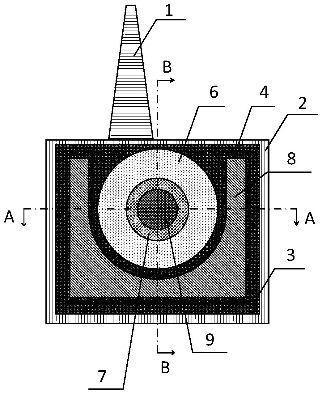
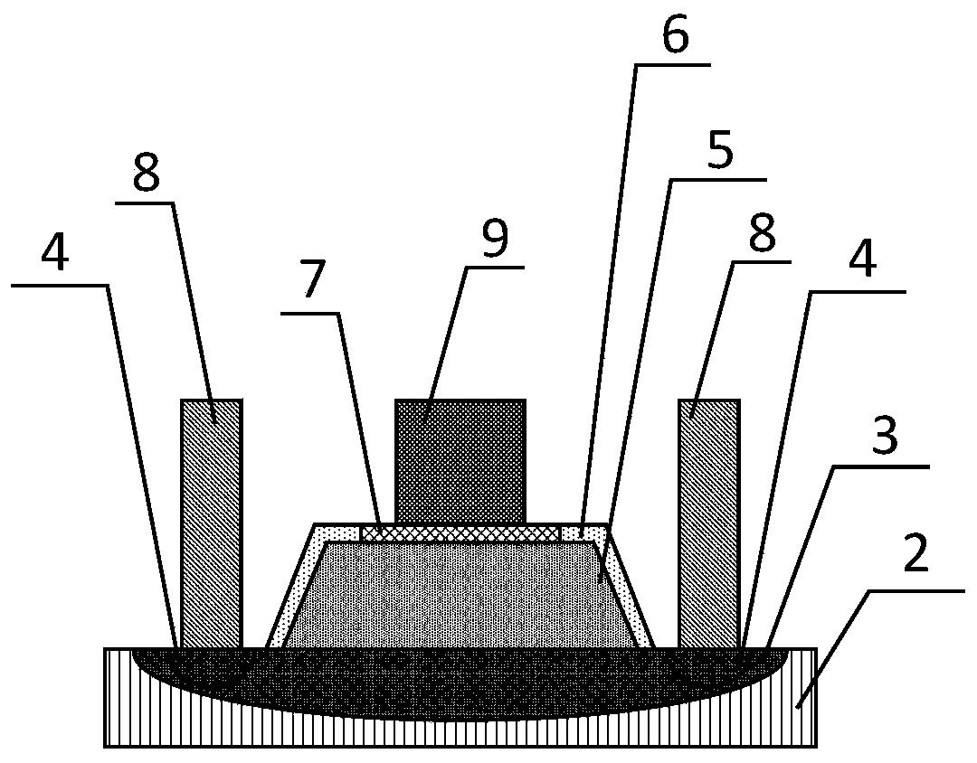
[0034] see Figure 1 to Figure 3 As shown, the embodiment of the present invention provides a silicon germanium photodetector with high bandwidth and high responsivity, including a silicon waveguide 1, a silicon substrate 2, a lightly doped silicon region 3, a heavily doped silicon region 4, and a germanium absorption region 5 , an epitaxial silicon region 6 , an epitaxial silicon doped region 7 , a first electrode 8 and a second electrode 9 .
[0035] The silicon waveguide 1 is used to transmit incident light; the silicon substrate 2 is used to receive the incident light transmitted by the silicon waveguide 1 and transmit it to the germanium absorption region 5; the lightly doped silicon region 3 is arranged in the silicon substrate 2, The lightly doped silicon region 3 is doped and diffused from the surface of the silicon substrate 2 to the inside of the silicon substrate 2; the heavily doped silicon region 4 is located in the lightly doped silicon region 3, and the heavily ...
Embodiment 2
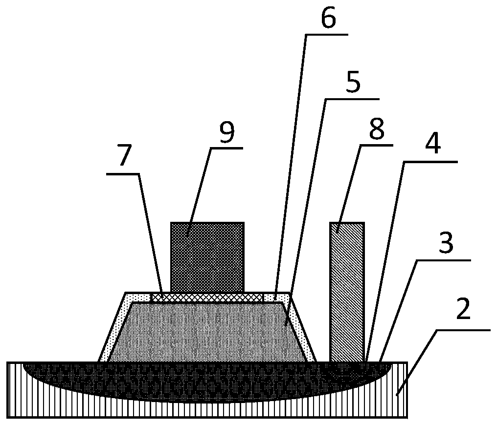
[0044] see Figure 4 As shown, the difference between the embodiment of the present invention and the first embodiment is that the germanium absorption region 5 includes a second part close to the silicon waveguide 1, and the projection of the second part on the lightly doped silicon region 3 The surface is square, so that the incident light has a larger incident absorption cross section in the germanium absorption region 5, more light enters the germanium absorption region 5, and the responsivity is improved.
PUM
 Abstract
Description
Claims
Application Information