Solder resist layer manufacturing method, printed circuit board manufacturing method and printed circuit board

A printed circuit board and manufacturing method technology, applied in the directions of printed circuit manufacturing, printed circuit, printed circuit secondary processing, etc., can solve the problems of easy falling off, affecting processing, and the solder mask is not flat enough.

Inactive Publication Date: 2020-04-21
SHANGHAI MEADVILLE ELECTRONICS
View PDF3 Cites 6 Cited by
  • Summary
  • Abstract
  • Description
  • Claims
  • Application Information

AI Technical Summary

Problems solved by technology

However, the original solder resist layer is not smooth enough, which will affect the subsequent processing, and it is easy to fall off.

Method used


Image

  • Solder resist layer manufacturing method, printed circuit board manufacturing method and printed circuit board
  • Solder resist layer manufacturing method, printed circuit board manufacturing method and printed circuit board
  • Solder resist layer manufacturing method, printed circuit board manufacturing method and printed circuit board

Examples


Embodiment Construction

[0042] The present invention is described in detail below in conjunction with accompanying drawing:

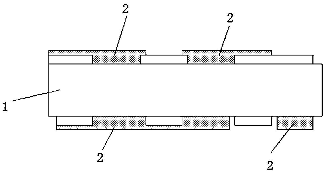
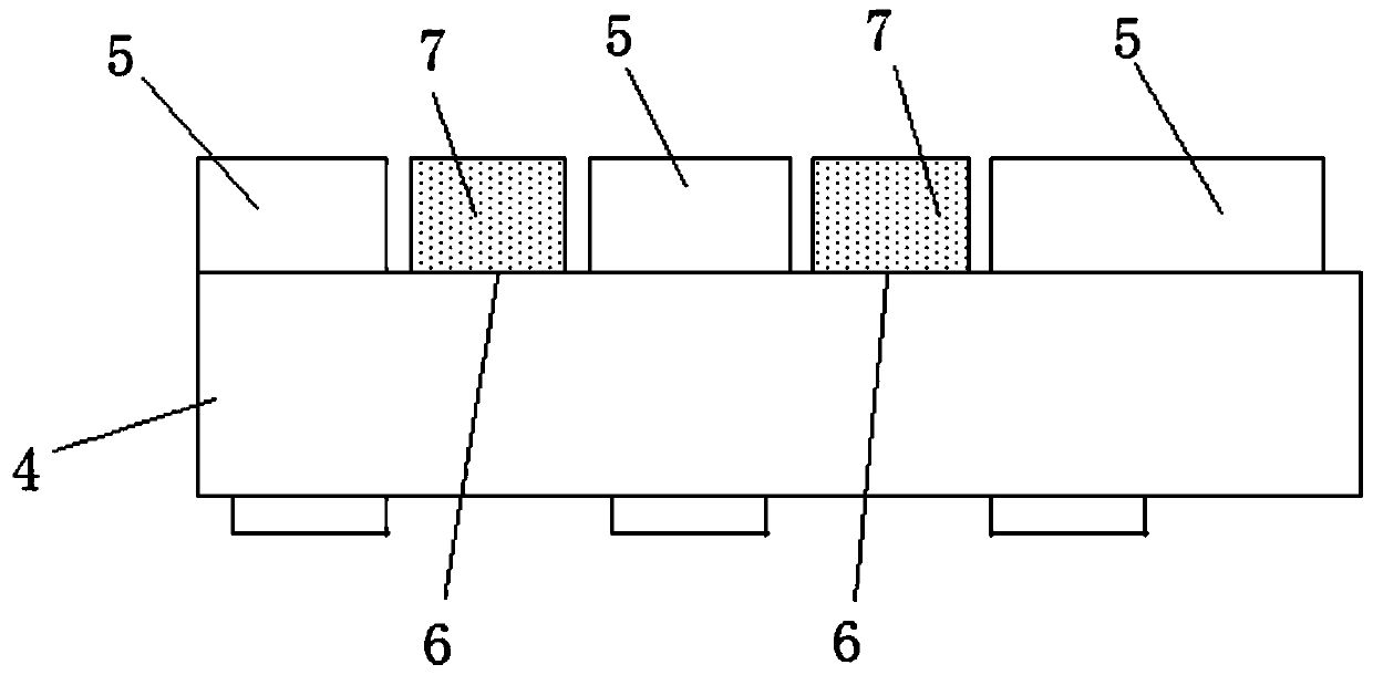
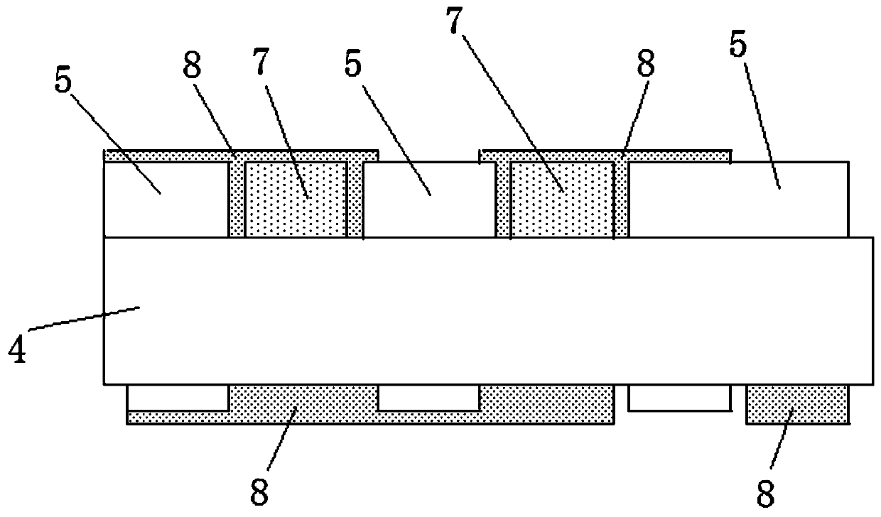
[0043] Such as figure 2 and image 3 As shown, the manufacturing method of the solder resist layer of the present embodiment, the manufacturing method of the printed circuit board and the printed circuit board, the manufacturing method of the solder resist layer include the following steps: The gap 6 between is filled with ink, namely figure 2 The shown ink fills up 7; Step 2, then prints the solder resist pattern on the printed circuit board 4, that is, as image 3 A solder resist layer 8 is fabricated as shown. The inks used in the present invention are conventional.

[0044] Such as figure 2 As shown, according to one embodiment of the present invention, the method for filling with ink described in step 1 includes the following steps:

[0045] a. Clean and activate the substrate of the printed circuit board 4; the step a uses plasma gas to activate the substrate ar...


PUM


Abstract

The invention discloses a solder resist layer manufacturing method, a printed circuit board manufacturing method and a printed circuit board. The solder resist layer manufacturing method comprises thefollowing steps: step 1, firstly, filling and leveling up a gap between thick copper on the printed circuit board by using printing ink; and step 2, performing solder resist pattern printing on the printed circuit board. The method of firstly filling and then solder resist is adopted. As the height difference between the base material area and the thick copper surface area is large, the lower base material area is firstly filled and leveled up by using solder resist ink, i.e., the height is basically equal to that of the thick copper surface, and then solder resist manufacturing is completedby using whole board ink printing so that the overall flatness of board surface ink is ensured; meanwhile, the etching amount of the ink side wall on the side of the base material area is reduced, thebinding force of the ink and the base material surface is increased, and ink falling can be prevented.

Description

technical field [0001] The invention relates to a method for manufacturing a solder resist layer, a method for manufacturing a printed circuit board and a printed circuit board. Background technique [0002] Such as figure 1 As shown, in the production of printed circuit boards (Printed Circuit Board, PCB), the outer layer must be made of solder mask. The function of the solder mask layer is to prevent the parts that should not be soldered from being connected by solder. Reflow soldering is realized by the solder mask layer. . The entire surface of the board is hot tin water, and the exposed circuit board without the solder mask will be soldered with tin, while the part with the solder mask will not be tin-stained. In addition, it also improves the insulation of lines or pads, prevents oxidation, and is more beautiful. However, the original solder resist layer is not smooth enough, which will affect the subsequent processing, and has the problem of easy falling off. Con...

Claims


Application Information

Patent Timeline
Patent Type & Authority Applications(China)
IPC IPC(8): H05K3/28
CPCH05K3/282
Inventor 刘涌王红月黄伟陈晓峰胡菊红
Owner SHANGHAI MEADVILLE ELECTRONICS
Why Eureka
Try Eureka