High-sensitivity nanowire acceleration sensor
An acceleration sensor, high-sensitivity technology, applied in the direction of acceleration measurement using inertial force, nanotechnology, nanotechnology, etc., can solve the problems of slender nanowire structure, and achieve the effect of easy deformation, small size, and low power consumption
- Summary
- Abstract
- Description
- Claims
- Application Information
AI Technical Summary
Problems solved by technology
Method used
Image

Examples
Embodiment 1
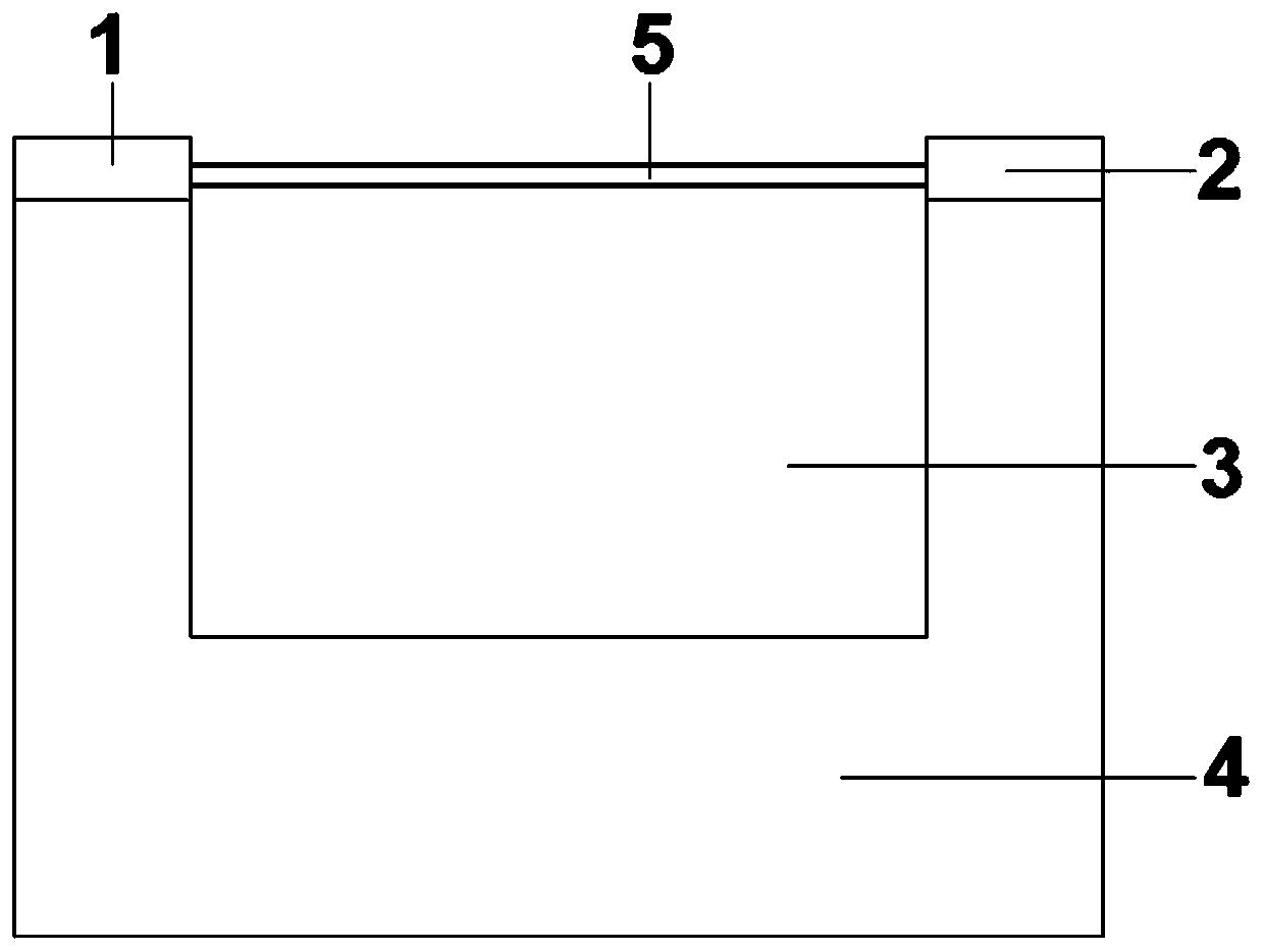
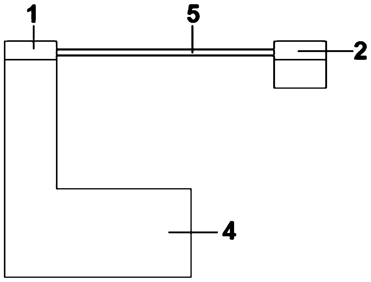
[0024] Such as figure 1 with figure 2 Shown as follows: First, using chemical vapor deposition (CVD) technology, an n-type GaN conductive layer with a thickness of 1-10 microns is grown on the surface of the sapphire substrate 4, and then the groove 3 is etched on the surface of the substrate 4. The groove 3 penetrates the conductive layer, so that the conductive layer is separated into a conductive layer a1 and a conductive layer b2 (that is, the conductive layer a1 and the conductive layer b2 are distributed on both sides of the groove 3, and the two are electrically insulated).
[0025] Secondly, GaN nanowires 5 are bridged and grown on the sidewalls of the groove 3. The nanowire 5 is in a suspended state and serves as a conductive channel for the conductive layer a1 and the conductive layer b2 on both sides of the groove 3, and connects the conductive layer a1 and the conductive layer b2 on both sides of the groove 3.
[0026] Next, the conductive layer 1a on the side of the g...
Embodiment 2
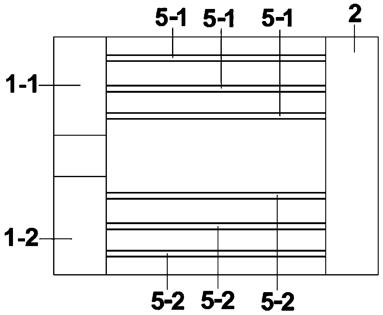
[0030] Such as figure 1 with Figure 5 Shown as follows: First, using chemical vapor deposition (CVD) technology, an n-type silicon conductive layer with a thickness of 1-10 microns is grown on the surface of the sapphire substrate 4, and then the groove 3 is etched on the surface of the substrate 4. The groove 3 penetrates the conductive layer, so that the conductive layer is separated into mutually insulated conductive layers a 3 1-3, conductive layer a 4 1-4, conductive layer a 5 1-5 and conductive layer a 6 1-6. Among them, the conductive layer a 3 1-3 and conductive layer a 4 1-4 are distributed on the opposite sides of annular groove 6, conductive layer a 5 1-5 and conductive layer a 6 1-6 are distributed on the other opposite sides of the annular groove 6.
[0031] Secondly, GaN nanowires are bridged and grown on the sidewalls of the annular groove 6 b 1 8-1 and nanowire b 2 8-2, the nanowire is suspended. Among them, nanowire b 1 8-1 Connect the conductive layer a 5 1-5 ...
PUM
 Abstract
Description
Claims
Application Information
 - R&D
- Intellectual Property
- Life Sciences
- Materials
- Tech Scout
- Unparalleled Data Quality
- Higher Quality Content
- 60% Fewer Hallucinations
Browse by: Latest US Patents, China's latest patents, Technical Efficacy Thesaurus, Application Domain, Technology Topic, Popular Technical Reports.
© 2025 PatSnap. All rights reserved.Legal|Privacy policy|Modern Slavery Act Transparency Statement|Sitemap|About US| Contact US: help@patsnap.com