Perovskite light emitting diode
A light-emitting diode and perovskite technology, applied in semiconductor devices, electrical components, circuits, etc., can solve the problems affecting light-emitting efficiency, light loss, etc., and achieve the effect of improving light-emitting efficiency, improving life and reliability, and high efficiency
- Summary
- Abstract
- Description
- Claims
- Application Information
AI Technical Summary
Problems solved by technology
Method used
Image


Examples
Embodiment 1
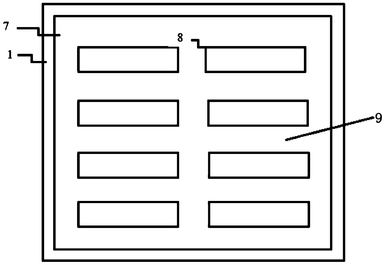
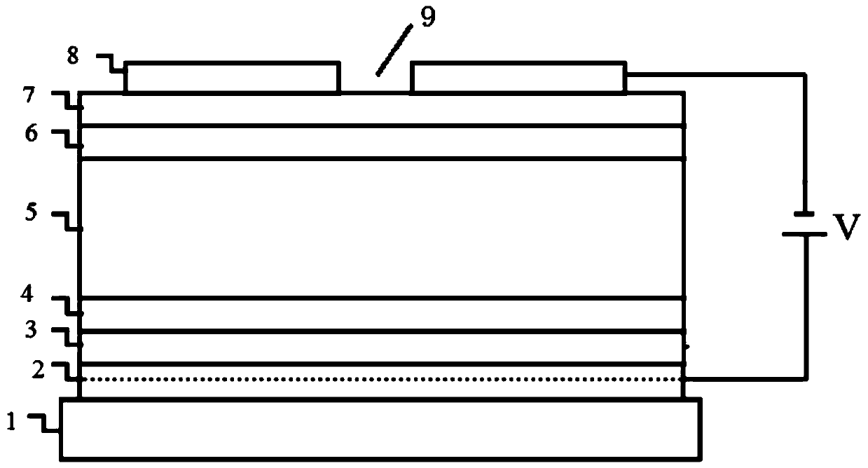
[0033] A perovskite light-emitting diode structure, from the bottom to the top structure is a substrate 1, a P-type electrode 2, a hole transport layer 3, a perovskite active light-emitting region 4, an electron transport layer 5, a mirror layer 6, The protective layer 7, the N-type electrode 8, the P-type electrode 2 is prepared on the substrate, the N-type electrode 8 is prepared on the protective layer, and an air channel 9 is left between a plurality of N-type electrodes 8; the P-type electrode 2 and the N-type The electrodes 8 are respectively connected to the positive pole and the negative pole of the external power supply.
[0034] In this embodiment, the substrate 1 is made of glass material; the thickness is 0.5 mm; the P-type electrode 2 is made of ITO material; prepared by spin coating; the thickness is 100 nm; the hole transport layer 3 is made of PEDOT:PSS; prepared by spin coating The thickness is 50nm; the perovskite active light-emitting region 4 is made of per...
Embodiment 2
[0036] A perovskite light-emitting diode structure, from the bottom to the top structure is a substrate 1, a P-type electrode 2, a hole transport layer 3, a perovskite active light-emitting region 4, an electron transport layer 5, a mirror layer 6, The protective layer 7, the N-type electrode 8, the P-type electrode 2 is prepared on the substrate, the N-type electrode 8 is prepared on the protective layer, and an air channel 9 is left between a plurality of N-type electrodes 8; the P-type electrode 2 and the N-type The electrodes 8 are respectively connected to the positive pole and the negative pole of the external power supply.
[0037] In this embodiment, the substrate 1 is made of glass material; the thickness is 1 mm; the P-type electrode 2 is made of ITO material; it is prepared by spin coating; the thickness is 150 nm; the hole transport layer 3 is made of TFB; it is prepared by spin coating; 100nm; the perovskite active light-emitting region 4 is made of two-dimensiona...
Embodiment 3
[0039] A perovskite light-emitting diode structure, from the bottom to the top structure is a substrate 1, a P-type electrode 2, a hole transport layer 3, a perovskite active light-emitting region 4, an electron transport layer 5, a mirror layer 6, The protective layer 7, the N-type electrode 8, the P-type electrode 2 is prepared on the substrate, the N-type electrode 8 is prepared on the protective layer, and an air channel 9 is left between a plurality of N-type electrodes 8; the P-type electrode 2 and the N-type The electrodes 8 are respectively connected to the positive pole and the negative pole of the external power supply.
[0040] In this embodiment, the substrate 1 is made of glass material; the thickness is 0.75 mm; the P-type electrode 2 is made of ITO material; it is prepared by spin coating; the thickness is 150 nm; the hole transport layer 3 is PVK; it is prepared by spin coating; 75nm; the perovskite active light-emitting region 4 is made of three-dimensional pe...
PUM
| Property | Measurement | Unit |
|---|---|---|
| Thickness | aaaaa | aaaaa |
| Thickness | aaaaa | aaaaa |
| Thickness | aaaaa | aaaaa |
Abstract
Description
Claims
Application Information
PatSnap Eureka turns technology decisions into work you can execute. Powered by our Innovation Knowledge Graph, it runs expert workflows across engineering, life sciences, materials and intellectual property. Get your review-ready output in minutes.


