High-speed low-voltage electrooptical modulator based on lithium niobate-silicon wafer

An electro-optical modulator, lithium niobate technology, applied in instruments, optics, nonlinear optics, etc., can solve the problems that pure silicon-based modulators are difficult to meet high speed, low voltage and low loss, achieve high refractive index, avoid etching , the effect of compact device

Active Publication Date: 2020-05-19
SHANGHAI JIAO TONG UNIV +1
View PDF4 Cites 8 Cited by
  • Summary
  • Abstract
  • Description
  • Claims
  • Application Information

AI Technical Summary

Problems solved by technology

However, with the development of optical fiber communication technology, it is difficult for pure silicon-based modulators to meet the requirements of high speed, low voltage, and low loss.

Method used


Image

  • High-speed low-voltage electrooptical modulator based on lithium niobate-silicon wafer
  • High-speed low-voltage electrooptical modulator based on lithium niobate-silicon wafer
  • High-speed low-voltage electrooptical modulator based on lithium niobate-silicon wafer

Examples


Embodiment 1

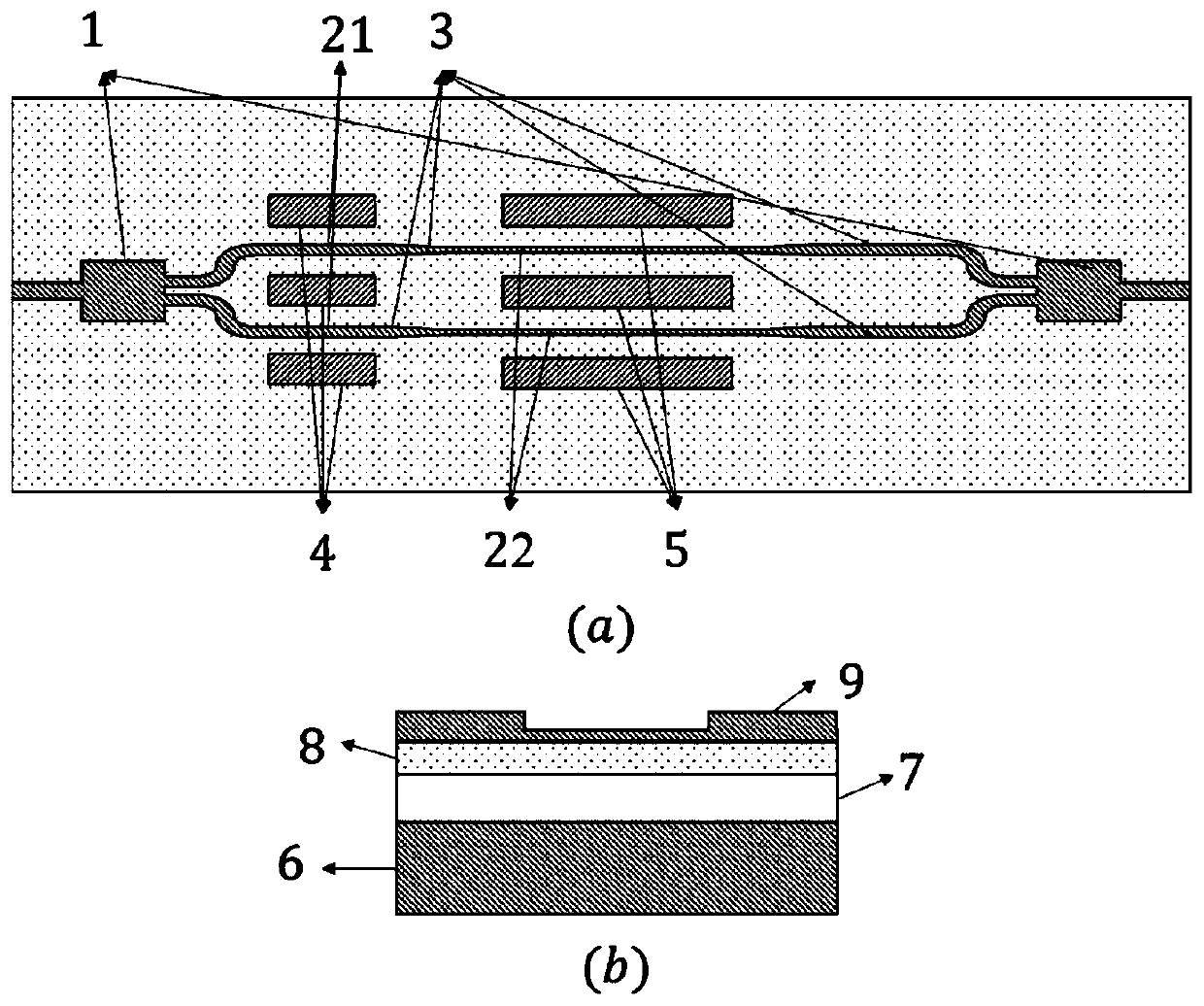
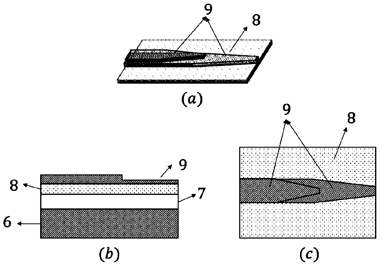
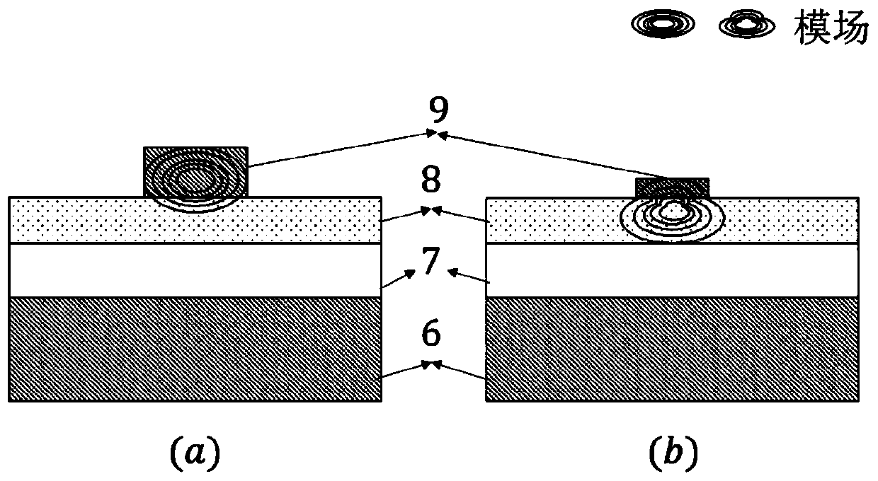
[0029]The basic structure of the present invention is a Mach-Zehnder modulator, including two multimode interferometers 1, two mode-spot converters 3, two thermally adjustable phase-shifting arms 21, two electrically adjustable phase-shifting arms 22, a DC bias Electrode 4 and RF electrode 5. The multimode interferometer is a 1×2 multimode interferometer, and the two multimode interferometers 1 serve as a wave combiner and a wave splitter respectively. The two output ports of the multiplexer are respectively connected to two thermally adjustable phase-shifting arms 21, and the two thermally adjustable phase-shifting arms 21 are respectively connected to one end of two mode-spot converters 3, and the two mode-spot converters 3 The other ends are respectively connected to two electrically controlled phase-shifting arms 22, and the two electrically controlled phase-shifting arms 22 are respectively connected to two modulus converters, and the two modulus converters 3 are finally ...

Embodiment 2

[0031] For the bias point control method of the high-speed, low-voltage modulator, in the embodiment of the present invention, the thermally adjustable phase-shift arm 21 is located in the high-refractive index region, and is used for the bias point control of the high-speed, low-voltage modulator. Therefore, from one port of the modulator to the other port, the waveguide structure components are the multimode interferometer 1 , the thermally tuned phase-shifting arm 21 , the mode-spot converter 3 , the electrically tuned phase-shifting arm 22 , and the multimode interferometer 1 .

Embodiment 3

[0033] In another embodiment of the present invention, the thermal phase shifter 21 is located in the low-refractive index region for bias point control of a high-speed, low-voltage modulator. Therefore, from one port of the modulator to the other port, the waveguide structure components are the multimode interferometer 1, the mode speckle converter 3, the thermal phase shifter 21, the electrical phase shifter 22, and the multimode interferometer 1.


PUM


Abstract

According to the high-speed low-voltage electrooptical modulator based on the lithium niobate-silicon wafer, the silicon wafer is located above the lithium niobate wafer, the silicon waveguide is etched to form the lithium niobate-silicon mixed waveguide, and the structure of the silicon waveguide is changed to enable light waves to have different energy distributions in the lithium niobate-silicon mixed waveguide. When the silicon waveguide has more energy distribution, the silicon waveguide is suitable for realizing a compact wave splitting function, a wave combining function and a thermo-optical modulation function; and when the lithium niobate waveguide has higher energy distribution, the lithium niobate waveguide is suitable for realizing a high-speed and low-voltage electro-optical modulation function. The advantages of a lithium niobate material platform and a silicon material platform are brought into play respectively, and the method is suitable for high-speed low-voltage electro-optical modulation.

Description

technical field [0001] The invention belongs to the technical field of photonic heterogeneous integration, in particular to a high-speed and low-voltage electro-optical modulator on a lithium niobate-silicon wafer. [0002] technical background [0003] The electro-optic modulator is an important functional device in optical fiber communication. Its function is to load the electrical signal onto the optical signal, so as to realize signal transmission and processing in the optical domain. Using complementary metal-oxide-semiconductor integration technology, pure silicon-based modulators fabricated on silicon wafers are the most common modulators in optical signal processing systems. However, with the development of optical fiber communication technology, it is difficult for pure silicon-based modulators to meet the requirements of high speed, low voltage, and low loss. In recent years, thanks to the development of lithium niobate thin film preparation technology, replacing p...

Claims


Application Information

Patent Timeline
Patent Type & Authority Applications(China)
IPC IPC(8): G02F1/03G02F1/035G02F1/21
CPCG02F1/0305G02F1/035G02F1/21G02F1/217G02F1/225G02F2202/20G02F1/212
Inventor 邹卫文王静徐绍夫王兴军
Owner SHANGHAI JIAO TONG UNIV
Why Eureka
Try Eureka