Flip LED chip

An LED chip and flip-chip technology, applied in electrical components, circuits, semiconductor devices, etc., can solve the problems of light inconcentration, chip dispersion, poor light efficiency, etc., to eliminate the impact, improve the light output efficiency, and reduce the voltage effect.

Pending Publication Date: 2020-05-19
FOSHAN NATIONSTAR SEMICON
View PDF0 Cites 1 Cited by
  • Summary
  • Abstract
  • Description
  • Claims
  • Application Information

AI Technical Summary

Problems solved by technology

The surface of the general epitaxial layer structure will have unevenness during the process of crystal growth, which will cause the reflective layer 40 plated on the back to form a complete mirror surface, which will cause dispersion of the chip, and the light will not be concentrated. After packaging into white light , leading to poor light effect

Method used


Image

  • Flip LED chip
  • Flip LED chip
  • Flip LED chip

Examples


Embodiment 1

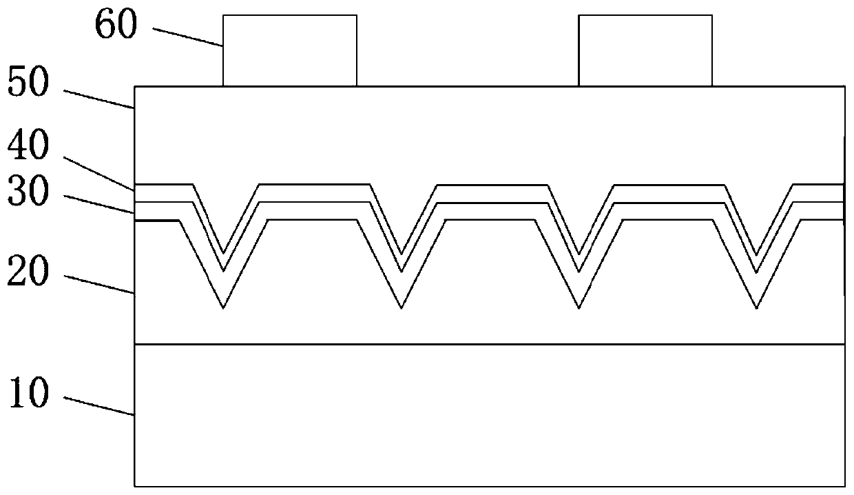
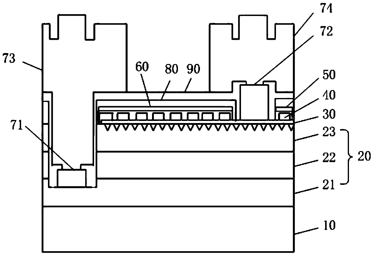
[0048] A flip-chip LED chip, comprising a substrate, an epitaxial layer, a transparent conductive layer, a leveling layer, an adhesive layer, a reflective layer, and an electrode structure, the epitaxial layer is arranged on the substrate, and the transparent conductive layer is arranged on On the epitaxial layer, the filling layer is arranged on the transparent conductive layer to fill up the concave-convex structure of the epitaxial layer, the filling layer is provided with a plurality of first holes, the adhesive layer is arranged on the filling layer and It is filled into the first hole to form a conductive connection with the transparent conductive layer. The reflective layer is arranged on the adhesive layer to form full mirror reflection. The filling layer is made of silicon oxide, and the adhesive layer is made of ITO. The reflective layer is made of silver, the thickness of the filling layer is 300nm, the thickness of the adhesive layer is 10nm, the thickness of the re...

Embodiment 2

[0050] A flip-chip LED chip, comprising a substrate, an epitaxial layer, a transparent conductive layer, a leveling layer, an adhesive layer, a reflective layer, and an electrode structure, the epitaxial layer is arranged on the substrate, and the transparent conductive layer is arranged on On the epitaxial layer, the filling layer is arranged on the transparent conductive layer to fill up the concave-convex structure of the epitaxial layer, the filling layer is provided with a plurality of first holes, the adhesive layer is arranged on the filling layer and Fill in the first hole to form a conductive connection with the transparent conductive layer, the reflective layer is arranged on the adhesive layer to form a total mirror reflection, the filling layer is made of aluminum oxide, and the adhesive layer is made of Ni / Made of Au oxide, the reflective layer is made of silver, the thickness of the filling layer is 500nm, the thickness of the adhesion layer is 30nm, the thicknes...

Embodiment 3

[0052] A flip-chip LED chip, comprising a substrate, an epitaxial layer, a transparent conductive layer, a leveling layer, an adhesive layer, a reflective layer, and an electrode structure, the epitaxial layer is arranged on the substrate, and the transparent conductive layer is arranged on On the epitaxial layer, the filling layer is arranged on the transparent conductive layer to fill up the concave-convex structure of the epitaxial layer, the filling layer is provided with a plurality of first holes, the adhesive layer is arranged on the filling layer and It is filled into the first hole to form a conductive connection with the transparent conductive layer. The reflective layer is arranged on the adhesive layer to form a total mirror reflection. The filling layer is made of magnesium difluoride, and the adhesive layer is made of Made of AzO, the reflective layer is made of silver, the thickness of the filling layer is 700nm, the thickness of the adhesive layer is 60nm, the t...


PUM

PropertyMeasurementUnit
thicknessaaaaaaaaaa
thicknessaaaaaaaaaa
diameteraaaaaaaaaa

Abstract

The invention discloses a flip LED chip, which comprises a substrate, an epitaxial layer, a transparent conductive layer, a filling and leveling layer, an adhesive layer, a reflecting layer and an electrode structure, wherein the epitaxial layer is arranged on the substrate; the transparent conductive layer is arranged on the epitaxial layer, the filling and leveling layer is arranged on the transparent conductive layer and fills the concave-convex structure of the epitaxial layer, the filling and leveling layer is provided with a plurality of first holes, the adhesion layer is arranged on thefilling and leveling layer and fills the first holes to form conductive connection with the transparent conductive layer, and the reflecting layer is arranged on the adhesion layer. The filling and leveling layer is formed on the transparent conductive layer of the flip LED chip; the concave-convex structure of the epitaxial layer is filled and leveled up to form a flat surface, and the reflecting layer arranged on the filling and leveling layer forms full mirror reflection, so that light emitted by the epitaxial layer can be emitted from the back surface of the substrate in a centralized manner after being reflected by the reflecting layer, and the light emitting efficiency of the chip is further improved.

Description

technical field [0001] The invention relates to the technical field of light emitting diodes, in particular to a flip-chip LED chip. Background technique [0002] see figure 1 , the existing flip-chip LED chip includes a substrate 10, an epitaxial layer 20 disposed on the front of the substrate 10, an ITO layer 30 disposed on the epitaxial layer 20, a reflective layer 40 disposed on the ITO layer 30, a reflective layer disposed on the reflective layer The insulating layer 50 on the 40, and the electrode 60. In the conventional flip chip, the light emitted from the side of the epitaxial layer 20 facing away from the substrate 10 is reflected by the reflective layer 40 and then emitted from the back side of the substrate 10 . The surface of the general epitaxial layer structure will have unevenness during the process of crystal growth, which will cause the reflective layer 40 plated on the back to form a complete mirror surface, which will cause dispersion of the chip, and t...

Claims


Application Information

Patent Timeline
Patent Type & Authority Applications(China)
IPC IPC(8): H01L33/46H01L33/42
CPCH01L33/42H01L33/46
Inventor 仇美懿庄家铭邓梓阳
Owner FOSHAN NATIONSTAR SEMICON
Why Eureka
Try Eureka