A full-gan integrated half-bridge dead-time adjustment circuit

A technology for adjusting circuits and dead time, applied in electrical components, high-efficiency power electronic conversion, and output power conversion devices, etc., can solve problems such as the design difficulty of full GaN digital circuits and the increase in process difficulty.

Active Publication Date: 2021-04-02
UNIV OF ELECTRONICS SCI & TECH OF CHINA
View PDF3 Cites 0 Cited by
  • Summary
  • Abstract
  • Description
  • Claims
  • Application Information

AI Technical Summary

Problems solved by technology

Traditional GaN gate circuits integrate depletion-mode devices and enhancement-mode devices together, which not only increases the difficulty of the process, but also because the depletion-mode devices are turned off by negative voltage, the driving circuit needs to output voltages of positive and negative polarities, which Brings difficulty to the design of all-GaN digital circuits

Method used


Image

  • A full-gan integrated half-bridge dead-time adjustment circuit
  • A full-gan integrated half-bridge dead-time adjustment circuit
  • A full-gan integrated half-bridge dead-time adjustment circuit

Examples


Embodiment approach

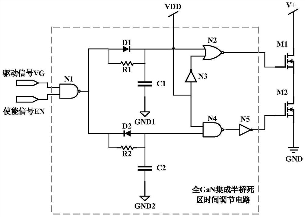
[0025] An embodiment of the present invention provides an all-GaN integrated half-bridge dead-time adjustment circuit, such as figure 1 As shown, it includes 2 NAND gate circuits N1 and N4, 1 NOR gate circuit N2, 2 NOT gate circuits N3 and N5, 2 diodes D1 and D2, 2 resistors R1 and R2, 2 capacitors C1 and C2.

[0026] The specific circuit structure has been described in detail in the content of the invention, and will not be repeated here.

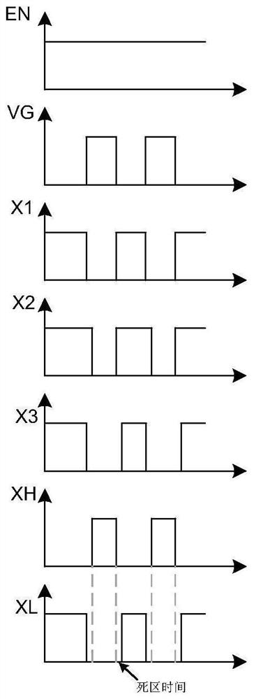
[0027] The working principle and process of the half-bridge circuit through protection circuit provided by the embodiment of the present invention will be described in detail below in conjunction with the accompanying drawings:

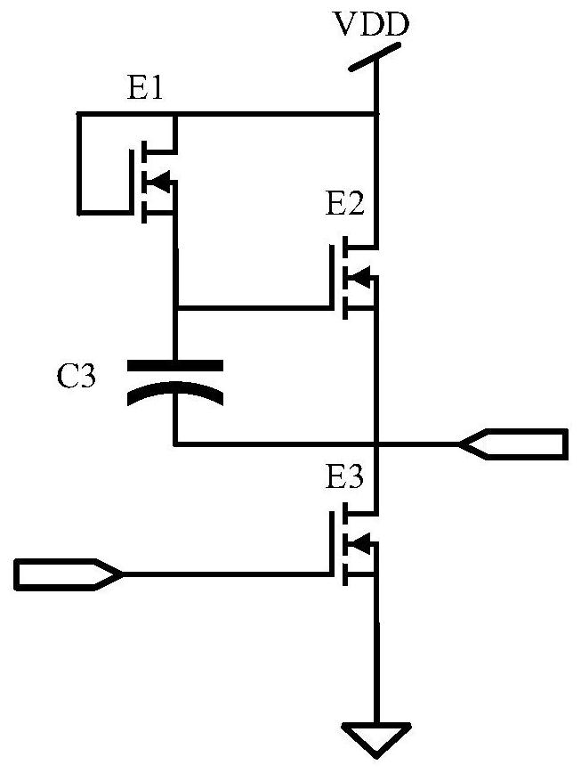
[0028] Such as image 3 As shown, the NOT gate circuit includes three transistors E1, E2 and E3, and one capacitor C3. When the voltage at the input terminal is low, the transistor E3 is in the off state, and the transistor E1 is in the on state because the gate and the drain are short-circuited, and the gate v...


PUM


Abstract

The invention discloses a full-GaN integrated half-bridge dead-time adjustment circuit, which realizes a full-GaN integrated basic digital logic gate circuit through an enhanced GaN power transistor, that is, a NOT gate circuit, an NAND gate circuit and an NOR gate circuit, and further Utilize these basic digital logic gates and GaN-based diodes to realize a full-GaN integrated half-bridge dead-time regulation circuit. The circuit effectively avoids the punch-through phenomenon caused by simultaneous opening of the high-side power device and the low-side power device in the half-bridge structure. At the same time, the dead time of the half-bridge structure is effectively adjusted by changing the resistance and capacitance. Lay the foundation for the industrialization of power-level full GaN integration.

Description

technical field [0001] The invention belongs to the technical field of GaN power devices, and in particular relates to the design of an all-GaN integrated half-bridge dead-time adjustment circuit. Background technique [0002] As a third-generation semiconductor material, GaN is widely used in the field of power electronics technology due to its excellent characteristics such as high breakdown electric field and high electron mobility. Compared with traditional Si devices, GaN HEMT power switching devices have the advantages of high frequency, high power density, and low loss in power conversion systems. After years of development, GaN power devices have become more and more widely used, ranging from automotive Lidar systems to consumer electronics chargers. [0003] The enhanced GaN device has three electrodes, which are the gate, the drain and the source, and its threshold voltage VTH is generally 0.5V to 2V. When the gate-source voltage VGS is greater than the threshold ...

Claims


Application Information

Patent Timeline
Patent Type & Authority Patents(China)
IPC IPC(8): H02M1/38
CPCH02M1/38H02M1/0012H02M1/385Y02B70/10
Inventor 周琦马骁勇明鑫
Owner UNIV OF ELECTRONICS SCI & TECH OF CHINA
Why Eureka
Try Eureka