Pixel structure, preparation method thereof and display panel

A pixel structure and pixel technology, which is applied in semiconductor/solid-state device manufacturing, semiconductor devices, electrical components, etc., can solve the problem of pixel arrangement that limits the printing method, increase equipment and time costs, and increase pixel aperture ratio Effect

Inactive Publication Date: 2020-05-26
SHENZHEN CHINA STAR OPTOELECTRONICS SEMICON DISPLAY TECH CO LTD
View PDF8 Cites 8 Cited by
  • Summary
  • Abstract
  • Description
  • Claims
  • Application Information

AI Technical Summary

Problems solved by technology

[0004] This disclosure provides a pixel structure, its preparation method, and a display panel, so as to alleviate the technical problem that the pixel arrangement of the existing mixed-arrangement OLED panel limits the printing method

Method used


Image

  • Pixel structure, preparation method thereof and display panel
  • Pixel structure, preparation method thereof and display panel
  • Pixel structure, preparation method thereof and display panel

Examples


Embodiment Construction

[0030] The following descriptions of the various embodiments refer to the accompanying drawings to illustrate specific embodiments in which the present disclosure may be practiced. The directional terms mentioned in this disclosure, such as [top], [bottom], [front], [back], [left], [right], [inside], [outside], [side], etc., are for reference only The orientation of the attached schema. Therefore, the directional terms used are used to explain and understand the present disclosure, but not to limit the present disclosure. In the figures, structurally similar elements are denoted by the same reference numerals.

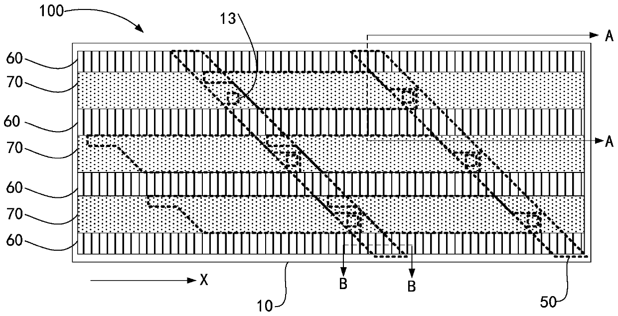
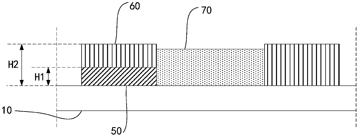
[0031] In one embodiment, as figure 2 As shown, a pixel structure 100 is provided, which includes a substrate 10 , a first pixel bank 50 and a second pixel bank 60 . The first pixel bank 50 is disposed on the substrate 10 and intersects the longitudinal direction X of the substrate 10 . The second pixel bank 60 is disposed on the substrate 10 across the first pixe...


PUM


Abstract

The invention provides a pixel structure, a preparation method thereof and a display panel. The pixel structure comprises a substrate, first pixel separation dikes and second pixel separation dikes, wherein the first pixel separation dikes are arranged on the substrate and intersect with the long side direction of the substrate; the second pixel separation dikes are arranged on the substrate across the first pixel separation dikes and are parallel to the long side direction of the substrate; and a light-emitting material of the same color is arranged between every two adjacent second pixel separation dikes, and the light-emitting materials cover part of the first pixel separation dikes. The pixel design can be compatible with Line-Bank printing in an MMG mode, and the problem that the printing mode is limited due to the pixel arrangement mode in an existing MMG is solved.

Description

technical field [0001] The disclosure relates to the field of display technology, and in particular to a pixel structure, a manufacturing method thereof, and a display panel. Background technique [0002] Organic Light Emitting Display (OLED) display has gradually become a high-end display replacing liquid crystal display due to its advantages such as ultra-high contrast, wide color gamut, fast response, and active light emission. As the size of OLED displays and OLED TVs continues to increase, the size of their corresponding mass-produced glass substrates also continues to increase. In order to maximize the utilization rate of glass, it is necessary to prepare OLED products of different sizes on the same glass substrate, that is, the mixed arrangement (MutiModel Group, MMG) technology. The traditional hybrid arrangement of OLED panels and pixel arrangement is as follows: figure 1 As shown, two types of OLED panels of different sizes, 65" and 55", are arranged on the same ...

Claims


Application Information

Patent Timeline
Patent Type & Authority Applications(China)
IPC IPC(8): H01L27/32H01L51/56
CPCH10K59/352H10K59/353H10K59/121H10K71/00H10K59/122H10K50/813H10K59/1201
Inventor 韩志斌
Owner SHENZHEN CHINA STAR OPTOELECTRONICS SEMICON DISPLAY TECH CO LTD
Why Eureka
Try Eureka