LED detection device and method

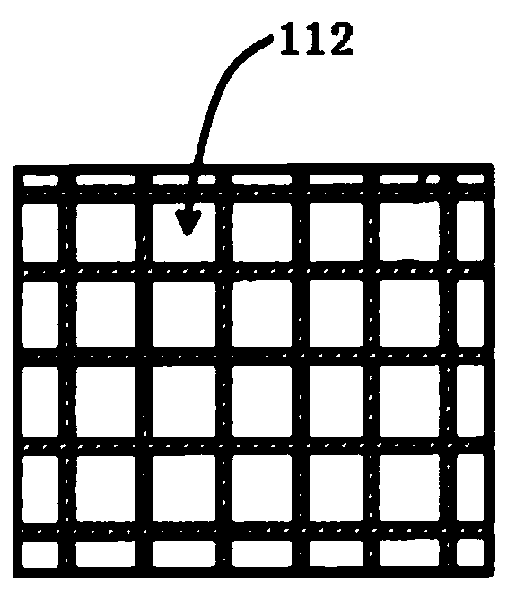
A detection device, LED chip technology, applied in semiconductor/solid-state device testing/measurement, electrical components, semiconductor/solid-state device manufacturing, etc., can solve problems such as puncturing LED112, slow LED chip detection, and difficulty in ensuring probes

Active Publication Date: 2020-05-26
CHONGQING KONKA PHOTOELECTRIC TECH RES INST CO LTD
View PDF9 Cites 6 Cited by
  • Summary
  • Abstract
  • Description
  • Claims
  • Application Information

AI Technical Summary

Problems solved by technology

Therefore, for Micro-LEDs, the size of the LED112 is very small, and it is difficult to align the probes with the electrodes of the LED112. In the process of using the probes to energize the LED chip on the chip substrate, there is a risk of stabbing the LED112, and it is difficult to Ensure that the probe can be accurately aligned with the electrodes of the LED chip
In addition, the traditional LED inspection method needs to move the position of the probe mechanically, resulting in a slow LED chip inspection speed

Method used


Image

  • LED detection device and method
  • LED detection device and method
  • LED detection device and method

Examples


Embodiment Construction

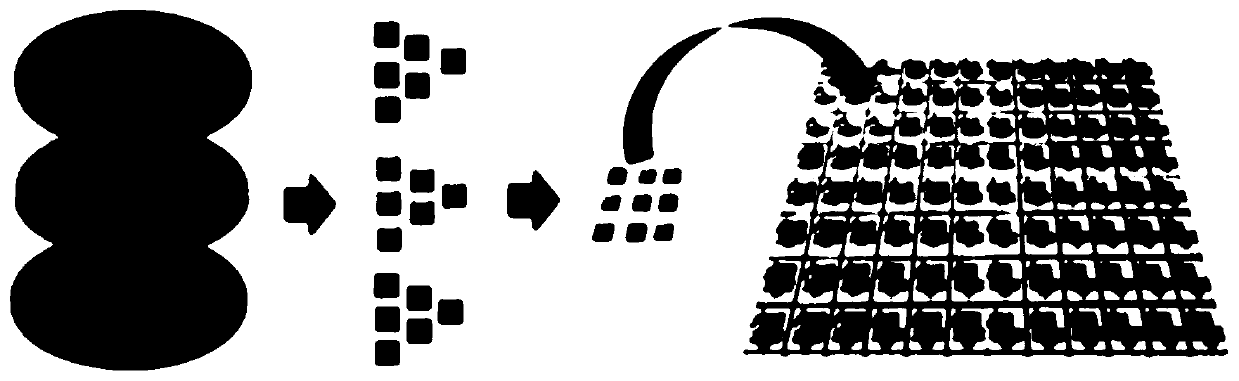
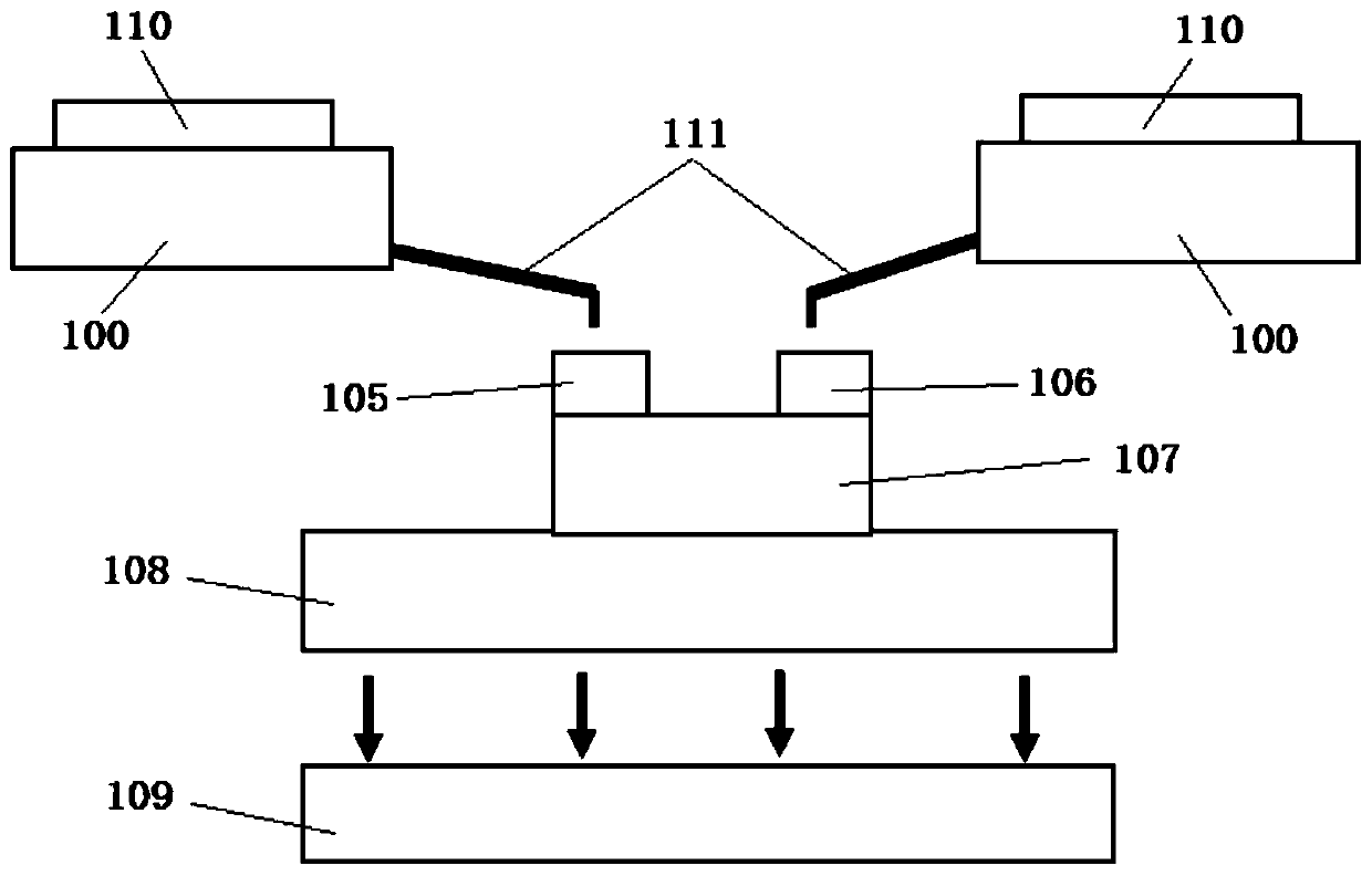
[0043] The invention provides an LED detection device and method. The LED detection device can manufacture corresponding detection electrode positions for LED chips of different sizes to perform electrical detection, and can perform electrical detection for LED chips with different heights. In order to make the object, technical solution and effect of the present invention more clear and definite, the present invention will be further described in detail below with reference to the accompanying drawings and examples. It should be understood that the specific embodiments described here are only used to explain the present invention, not to limit the present invention.

[0044] In the embodiments and the scope of the patent application, unless there is a special limitation on the article, "a" and "the" can generally refer to a single or plural.

[0045] In addition, if there are descriptions involving "first", "second" and so on in the embodiments of the present invention, the d...


PUM


Abstract

The invention discloses an LED detection device and method. The LED detection device comprises a detection circuit board; an elastic substrate arranged at the lower end of the detection circuit board,wherein a detection electrode is arranged on the face, away from the detection circuit board, of the elastic substrate, the detection electrode is electrically connected with the detection circuit board, and the detection electrode is right opposite to an electrode of a to-be-detected LED chip; and a fillable area, wherein the fillable area is arranged between the detection circuit board and theelastic substrate. According to the invention, after the fillable area is filled, the detection electrode is in contact with the to-be-detected electrode to judge whether the to-be-detected LED chip at the current detection position is a chip with poor electrical property or not, so that the chip with poor electrical property can be screened out. Besides, the position of a probe does not need to be moved mechanically, the LED chip is prevented from being stabbed by the probe, the LED chip can be accurately aligned with an electrode of the LED chip to be powered on, and the detection speed of the LED chip is increased.

Description

technical field [0001] The present invention relates to the field of Micro-LED technology, in particular to an LED detection device and method. Background technique [0002] Micro-LED (Light Emitting Diode, LED) technology, that is, LED miniaturization and matrix technology. Micro-LED has good stability and advantages in operating temperature, and has a long service life. At the same time, it also inherits the advantages of LED such as low power consumption, color saturation, fast response speed, and strong contrast. In addition, Micro-LED has higher brightness and lower power consumption. [0003] Such as figure 1 As shown, due to lattice matching, LED micro-devices must first be grown on sapphire-like substrates by molecular beam epitaxy. To make a display, LED light-emitting micro-devices must be transferred to a glass substrate. Since the size of the sapphire substrate for making LED micro-devices is basically the size of a silicon wafer, and the size of a much large...

Claims


Application Information

Patent Timeline
Patent Type & Authority Applications(China)
IPC IPC(8): H01L21/66H01L21/67
CPCH01L22/14H01L21/67271
Inventor 钟光韦伍凯义杨然翔江仁杰沈佳辉
Owner CHONGQING KONKA PHOTOELECTRIC TECH RES INST CO LTD
Why Eureka
Try Eureka