
Optical digital-to-analog converter, signal processing system and photonic neural network chip

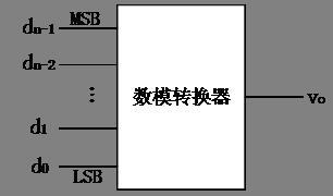
A digital-to-analog converter and photoelectric converter technology, which is applied in the field of photonic computing and can solve the problems of inability to realize all-optical computing, high price, and difficulty in amplifiers.

Active Publication Date: 2020-05-29
光子算数(北京)科技有限责任公司
View PDF6 Cites 3 Cited by
  • Summary
  • Abstract
  • Description
  • Claims
  • Application Information

AI Technical Summary

Problems solved by technology

But up to now, the three key indicators of bandwidth, sampling rate and quantization accuracy of digital-to-analog converters based on electronic technology are close to the physical limit, and it is difficult to achieve further improvement on the original architecture.
At the same time, high-precision, high-speed digital-to-analog converters are restricted by foreign countries, and high-speed digital-to-analog converters and analog-to-digital converters with frequencies up to GHz are very expensive in the market
[0003] As a technology completely different from electronic computing, optical computing uses photons as the information processing carrier, relies on optical hardware instead of electronic hardware, replaces electrical computing with optical computing, and can quickly process highly complex computing tasks in parallel. However, the current photon Chips still cannot achieve all-optical computing, and still need to cooperate with electronic chips
In the process of cooperation between photonic chips and electronic chips, it is necessary to face the technical problem of converting the digital signal of the electronic chip into the analog optical signal required by the photonic chip, and because it is difficult to make an amplifier on the silicon base, the digital-to-analog converter on the light suffers from technical difficulties. bottleneck

Method used


Image

  • Optical digital-to-analog converter, signal processing system and photonic neural network chip
  • Optical digital-to-analog converter, signal processing system and photonic neural network chip
  • Optical digital-to-analog converter, signal processing system and photonic neural network chip

Examples


Embodiment Construction

[0027] The technical solutions in the embodiments of the present application will be described below with reference to the drawings in the embodiments of the present application.

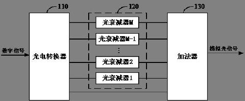
[0028] Photon computing uses light to provide computing power, which can significantly improve computing power. At the same time, since optical signals are used to replace electronic signals on silicon chips to transmit data, the signal transmission speed can be greatly improved and power consumption can be reduced. In view of the fact that photonic chips have huge advantages in terms of calculation rate and power consumption compared with traditional electronic digital processing chips, and current photonic chips still need to rely on cooperation with electronic chips, this embodiment thus provides a Optical digital-to-analog converter. The electrical chip processes digital signals, while the photonic chip processes analog optical signals. Therefore, the signal transmission between the electrical c...


PUM


Abstract

The invention provides an optical digital-to-analog converter, a signal processing system and a photonic neural network chip. The optical digital-to-analog converter comprises a photoelectric converter which is used for receiving N bits of digital signals transmitted by an electric chip, converting each bit of data in the digital signals into a corresponding optical signal and outputting N paths of optical signals corresponding to the digital signals in parallel, and N is a positive integer; a optical attenuator group, used for receiving N-1 paths of optical signals in the N paths of optical signals and attenuating the N-1 paths of optical signals to obtain N-1 paths of attenuated optical signals; and an adder, used for adding the N-1 paths of attenuation optical signals and one path of optical signals except the N-1 paths of optical signals in the N paths of optical signals to obtain an analog optical signal. According to the optical digital-to-analog converter, the optical attenuatorset is used for attenuating optical signals, the analog quantity of the output analog optical signals is in direct proportion to the digital quantity of the input digital signals after the optical signals pass through the optical digital-to-analog converter, and conversion from the digital quantity to the analog quantity is achieved.

Description

technical field [0001] The present application relates to the technical field of photonic computing, in particular, to an optical digital-to-analog converter, a signal processing system and a photonic neural network chip. Background technique [0002] A digital-to-analog converter is a device that converts digital signals into analog signals. In many electronic circuits, signals are stored and transmitted digitally, and digital-to-analog converters can convert such signals into analog signals, so that these signals Can be recognized by the outside world (including people or external devices). The digital-to-analog converter is a bridge connecting the analog world and the digital world. In the current era of information explosion, in order to meet the needs of users for massive data and the requirements for information quality in various fields, digital-to-analog converters continue to move towards higher speeds and higher Development in the direction of high precision. But...

Claims


Application Information

Patent Timeline
IPC IPC(8): G02F7/00G06N3/067
CPCG02F7/00G06N3/0675
Inventor 赵斌白冰李智吴建兵
Owner 光子算数(北京)科技有限责任公司
Learn More